5 Domestic and Overseas Wafer Factories and 2 Packaging Factories
"This Year's In-House 3-Nanometer Production Capacity Tripled Compared to Last Year"
"$1 Trillion Global Semiconductor Production Value by 2030"
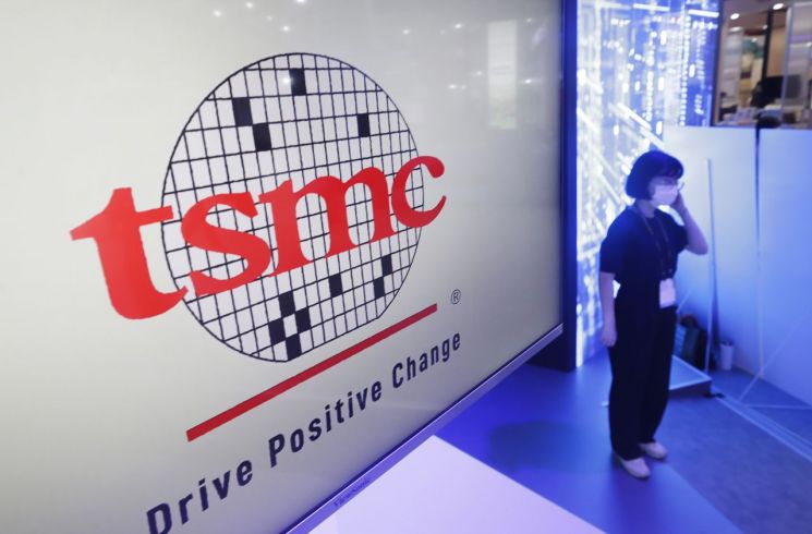
TSMC, the world's No. 1 foundry (semiconductor contract manufacturing) company, plans to strengthen its semiconductor production capacity by constructing seven additional factories this year, according to Taiwanese local media such as China Times on the 24th.
According to the report, Huang Yuan-guo, Senior Factory Manager of TSMC's 18B fab (semiconductor production plant) located in Tainan, southern Taiwan, stated at a technology symposium held in Taipei, Taiwan, the day before, "To meet customer demand, we plan to build a total of seven factories domestically and internationally this year, including two overseas fabs and packaging plants."
Senior Factory Manager Huang explained the background of the factory expansion, saying, "Our 3㎚ (nanometer; 1㎚ = one billionth of a meter) process production capacity has tripled compared to last year," but "supply still cannot keep up with demand."
Another official pointed to the increased demand for high-performance computing (HPC) and flagship smartphones as the cause of the 3-nanometer product supply shortage. The official predicted, "Apple's A18 processor, Qualcomm's Snapdragon 8 Gen 4, and MediaTek Dimensity 9400 are highly likely to adopt TSMC's 3-nanometer second-generation process N3E products, which will further exacerbate the supply shortage."
Senior Factory Manager Huang stated, "The packaging plant Taichung Fab 5 (AP5) will start mass production using an advanced process called 'Chip on Wafer on Substrate' (CoWoS) from 2025, and the Tainan Fab 7 (AP7) plans to begin mass production using CoWoS and SoIC (System On Integrated Chips) from 2026." SoIC is TSMC's semiconductor packaging brand, characterized by making electronic pathways thinner and reducing the distance between chips compared to traditional packaging methods, thereby increasing data transmission speeds.
This aggressive foundry expansion suggests that TSMC is positively evaluating the potential growth of the artificial intelligence (AI) industry. At this technology symposium, TSMC forecasted that AI accelerator demand will grow 2.5 times compared to last year. It also projected that the global semiconductor production value will reach $1 trillion (approximately 1,300 trillion KRW) by 2030, with foundry production accounting for $250 billion (approximately 340 trillion KRW) of that total.
TSMC Senior Vice President of Business Development Zhang Xiaochang reported that the construction progress of the 2-nanometer process is going smoothly and mass production is expected to begin in 2025. Nanometer refers to the unit indicating the width of semiconductor circuit lines; the narrower the line width, the lower the power consumption and the faster the processing speed. Currently, the world's most advanced mass production technology is 3 nanometers. In the 2-nanometer sector, TSMC is generally regarded as having an advantage in the industry.
© The Asia Business Daily(www.asiae.co.kr). All rights reserved.
