Competition for Leadership in Fine Process Intensifies
Market Leadership Strategy Through Enhanced Choice
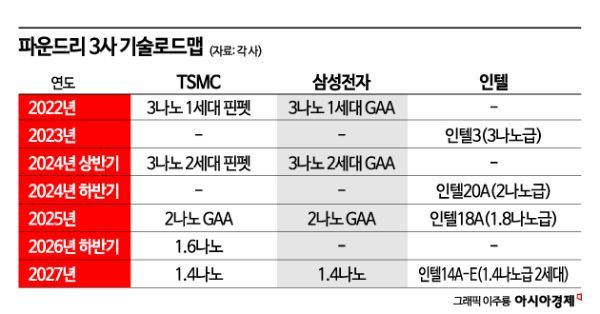
On the 24th (local time), Taiwan's TSMC, the world's No. 1 foundry (semiconductor contract manufacturing) company, made a surprise announcement that it plans to produce semiconductors using a 1.6㎚ (nanometer; 1㎚ is one billionth of a meter) process starting in the second half of 2026. TSMC had previously announced plans for 2㎚ in 2025 and 1.4㎚ in 2027, but there was no production plan using the 1.6㎚ process. Given that U.S. semiconductor company Intel recently mentioned a 1.8㎚ process, TSMC's announcement is widely interpreted as targeting Intel.
Y.J. Mi, Co-Chief Operating Officer (COO) of TSMC, declared the '2026 1.6㎚' system at a technology conference held in Santa Clara, California, saying, "Power can be supplied from the back of the chip, which can increase the speed of artificial intelligence (AI) chips," and added, "This is a field where we compete with Intel."
Maintaining the goal of '1.4㎚ production in 2027' while announcing '1.6㎚ production' is evaluated as showing confidence that TSMC can maintain and manage yield stability and sufficiently protect its market share even if Intel and Samsung Electronics challenge it. Samsung Electronics also has plans for 2㎚ and 1.4㎚ processes similar to TSMC but does not have a 1.6㎚ process.
Kevin Zhang, Senior Vice President of Business Development at TSMC, did not specify particular customers but explained, "Due to demand from AI chip companies, we developed the new A16 chip manufacturing process faster than expected." The A16 chip refers to the 1.6㎚ process.
He added, "AI chip manufacturers are more likely to adopt this technology first rather than smartphone manufacturers," and "AI chip companies optimize chip design to maximize performance." He also mentioned, "It seems unnecessary to use ASML's new next-generation lithography equipment (High NA EUV) for the A16 process."
Intel announced on the 18th that it installed this equipment at its research and development (R&D) center in Oregon, USA. It was the first foundry company to introduce the 'High NA EUV' equipment.
TSMC's declaration of 1.6㎚ production is a strategic move to secure both customer trust and market leadership. It also means that while following the 1.4㎚ roadmap three years later, TSMC has the capability to provide flexible services according to changes in customer orders. This implies that TSMC has the leeway to conduct business by considering market demand, advanced process yield, and competitors' sales strategies.
This announcement is expected to intensify competition over leadership in fine process technology. Intel has declared its re-entry into the foundry business with ambitions to surpass Samsung and become the world's No. 2 by 2030. Samsung has also formalized plans for mass production of the 1.4㎚ process.
Professor Kwon Seok-jun of the Department of Chemical Engineering at Sungkyunkwan University, known as the author of the 'Semiconductor Three Kingdoms,' said, "Apart from the 1.4㎚ development plan, this is a strategy to adjust capacity while monitoring market demand and advanced process yield trends and to respond flexibly to large customer order fluctuations." He added, "It shows the market a bridging option to respond to the current significant slowdown in TSMC's No. 1 customer Apple’s mobile market situation and Nvidia's mass production volume."
© The Asia Business Daily(www.asiae.co.kr). All rights reserved.

![User Who Sold Erroneously Deposited Bitcoins to Repay Debt and Fund Entertainment... What Did the Supreme Court Decide in 2021? [Legal Issue Check]](https://cwcontent.asiae.co.kr/asiaresize/183/2026020910431234020_1770601391.png)


