Collaborating to Combine TSMC Packaging Technologies
SK Hynix is collaborating with Taiwanese foundry company TSMC to strengthen its capabilities not only in producing next-generation artificial intelligence (AI) memory semiconductors, specifically High Bandwidth Memory (HBM), but also in advanced packaging technologies. Through this partnership, ultra-fine processes will be introduced starting from the 6th generation HBM product, HBM4, to offer customized products tailored to customer requirements.
On the 19th, SK Hynix announced that it recently signed a memorandum of understanding (MOU) with TSMC in Taipei, Taiwan, regarding technological cooperation.
SK Hynix will collaborate with TSMC to develop HBM4, which is scheduled for mass production in 2026. The company stated, "By joining forces with TSMC, the leading foundry company, we will drive innovation in HBM technology," adding, "Based on three-way technological cooperation among customers, foundries, and memory, we will overcome the performance limits of memory."
The two companies will work on improving the performance of the base die, which is mounted at the bottom of the HBM package. HBM is created by vertically stacking core dies?DRAM single chips?on top of the base die and connecting them through silicon through-via (TSV) technology, which involves drilling tiny holes. The base die is connected to the graphics processing unit (GPU) and controls the HBM.
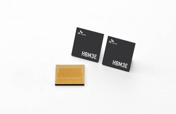
Until the 5th generation HBM3E, SK Hynix manufactured the base die using its own process, but starting with HBM4, it plans to utilize advanced logic processes. Applying ultra-fine processes in the base die production allows for the addition of various functions. According to the company, this enables the production of customized HBMs that meet a wide range of customer demands, including performance and power efficiency.
Additionally, the two companies will cooperate to optimize the combination of SK Hynix’s HBM and TSMC’s advanced packaging process, CoWoS (Chip on Wafer on Substrate). They also formalized plans to jointly respond to customer requests related to HBM. CoWoS is a packaging method that places the GPU and HBM on a special substrate and connects them. Since it combines logic chips on a horizontal (2D) substrate with vertically stacked (3D) HBM, it is referred to as 2.5D packaging.
Kim Ju-seon, President of SK Hynix, said, "Through collaboration with TSMC, we will not only develop the highest-performance HBM4 but also accelerate open collaboration with global customers," adding, "We will strengthen our competitiveness in customer-tailored memory platforms and solidify our position as a 'Total AI Memory Provider.'"
Kevin Zhang, Senior Vice President of TSMC, stated, "TSMC and SK Hynix have maintained a partnership for years, supplying AI solutions that combine leading-edge logic chips and HBM to the market," and added, "For HBM4 as well, the two companies will work closely to provide the best integrated products that will be key to customers’ AI-driven innovations."
© The Asia Business Daily(www.asiae.co.kr). All rights reserved.
![Clutching a Stolen Dior Bag, Saying "I Hate Being Poor but Real"... The Grotesque Con of a "Human Knockoff" [Slate]](https://cwcontent.asiae.co.kr/asiaresize/183/2026021902243444107_1771435474.jpg)

