Intel Hosts 'IFS Direct Connect'
Announces 1-Nanometer Foundry Process Roadmap
Also Reveals Order Strategies by Foundry Sector
American semiconductor company Intel announced that it will introduce the 1.8-nanometer (nm; 1 nm = one billionth of a meter) class 18A process in its foundry (semiconductor contract manufacturing) business within this year. In 2027, it plans to introduce the 1.4 nm process. With Taiwan's TSMC and Samsung Electronics also announcing plans to introduce the 1.4 nm process in 2027, Intel has taken the lead in the sub-nanometer process competition. Alongside this, Intel revealed a 'foundry order splitting' strategy that separately accepts packaging orders as well as chip production. Through this, it has set an ambitious goal to become the second-largest player in the foundry industry by 2030.
 Pat Gelsinger, Intel CEO, speaking at the 'IFS (Intel Foundry Service) Direct Connect' event held on the 21st (local time) in San Jose, California, USA / Photo by Intel
Intel to Introduce Industry's First 1-nm Class Process
On the 21st (local time), Intel held the ‘IFS (Intel Foundry Services) Direct Connect’ event at the McEnery Convention Center in San Jose, California, unveiling its advanced process roadmap plans. The IFS Direct Connect was held for the first time and was the first foundry event since Intel announced its re-entry into the foundry business in 2021, conducted with its partners.
The event was attended by Intel's key executives including CEO Pat Gelsinger, Microsoft (MS) CEO Satya Nadella, OpenAI CEO Sam Altman, as well as government officials such as U.S. Secretary of Commerce Gina Raimondo, and industry figures including Rene Haas, CEO of Arm, Eric Fischer, President of MediaTek, and Jason Wang, President of UMC.
Intel announced that it has secured four customers, including Microsoft, for the mass production of the 18A process within this year. It is reported that Microsoft has entrusted Intel with the production of its AI chip ‘Myia.’ CEO Gelsinger stated, "Only a few companies in the world can do this," and added, "Intel's 18A chips will surpass TSMC's processing speed."
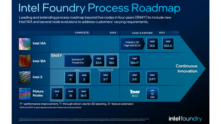
Intel's plan to mass-produce the 18A process is ahead of its original schedule, which aimed for production in 2025. If Intel's plan proceeds as scheduled, it will surpass TSMC and Samsung Electronics, who plan to introduce the 2 nm process next year.
Furthermore, Intel plans to introduce the 1.4 nm class 14A process starting in 2027. With TSMC and Samsung Electronics also announcing mass production of the 1.4 nm process in the same year, Intel has chosen to engage in a full-scale competition. To gain an edge in the fierce advanced process competition, Intel has become the first in the industry to adopt the next-generation extreme ultraviolet (EUV) lithography equipment ‘High Numerical Aperture (NA)’ from Dutch company ASML.
Based on this, Intel has set a goal to become the second-largest foundry company by 2030. While TSMC and Samsung Electronics currently hold the major market shares in the foundry market, Intel, which joined late, has expressed its ambition to take Samsung Electronics’ second place within six years through rapid process transitions.
Separating Production and Packaging... Revealing 'Foundry Order Splitting' Strategy
Intel also unveiled a ‘Systems Foundry’ strategy that splits foundry orders by sector. Unlike the traditional foundry business that handled chip production, packaging, and testing all at once, Intel plans to separate these to better respond to customer demands in each sector. For example, chips produced by TSMC could be packaged and finalized by Intel.
This is expected to be a measure to respond to the rapidly increasing demand for AI semiconductors. Recently, the industry has noted that the packaging production capacity of foundries like TSMC is insufficient compared to demand, causing delays in AI semiconductor production.
Demand for AI semiconductors is soaring to the point of causing supply bottlenecks. Jensen Huang, CEO of Nvidia, described the AI trend as a 'tipping point' during the fiscal year 2024 Q4 (November 2023 to January 2024) earnings announcement. He explained that with supply reaching its limits, even a slight increase in demand is sharply driving up AI semiconductor prices.
A semiconductor industry insider said, "As Intel expands its foundry business and starts accepting orders split by sector, this is a natural progression," adding, "If Intel's roadmap proceeds smoothly as planned, it will help increase its foundry market share."
Intensifying Competition in Advanced Foundry Processes
If Intel takes on some packaging demand, product supply in the market could accelerate. Samsung Electronics, which is expecting growth in AI-related business, will face even fiercer competition. However, Intel's relatively late adoption of EUV technology compared to TSMC and Samsung Electronics, following its re-entry into the foundry business in 2021, is considered a risk.
A semiconductor industry insider explained, "Since Intel did not previously utilize EUV equipment and is adopting it relatively late, there may be trial and error," adding, "EUV adoption is a highly challenging task, and the success or failure will affect whether the business expands."
Intel is showing confidence. CEO Gelsinger said on the day, "AI is changing the world," and added, "This will be an unprecedented opportunity for innovative chip designers and our foundry."
© The Asia Business Daily(www.asiae.co.kr). All rights reserved.
![Clutching a Stolen Dior Bag, Saying "I Hate Being Poor but Real"... The Grotesque Con of a "Human Knockoff" [Slate]](https://cwcontent.asiae.co.kr/asiaresize/183/2026021902243444107_1771435474.jpg)


