On the 31st, Sejong University announced that Professor Hong Young-jun of the Department of Nano New Materials Engineering, Professor Jang So-yeon of Seoul National University, and Professor Kim Dong-hwan of Sungkyunkwan University elucidated the principle of remote semiconductor epitaxy technology that allows easy separation from the substrate after growth through international joint research.
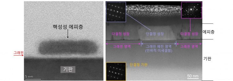 The principle of remote epitaxial growth technology for semiconductors.
 [Photo by Sejong University]
Remote epitaxy technology is a method of manufacturing a single-crystal semiconductor epitaxial layer with the same crystal orientation and structure as the substrate, using a substrate coated with two-dimensional materials such as graphene, without chemical bonding to the substrate.
The research team demonstrated that remote epitaxy is possible by stacking graphene layer by layer to compensate for micro-defects. Additionally, through experiments showing that adjusting the growth temperature on various substrates coated with graphene of the same quality changes the nucleation density of remote epitaxy, they proved that the interaction between the substrate and remote epitaxy exists, not micro-defects.
The results of this study, recognized for elucidating the principle of a novel semiconductor epitaxy manufacturing technology without chemical bonding, were published on the 20th in a convergence academic journal issued by the American Association for the Advancement of Science.
© The Asia Business Daily(www.asiae.co.kr). All rights reserved.


