Samsung Electronics Hosts 'Foundry Forum 2023'
Reveals Detailed Roadmap for 2nm Mass Production in 2025
Entry into 8-inch Gallium Nitride Power Semiconductor Market
Launch of Package Collaboration Group 'MDI Alliance'
Samsung Electronics has announced mass production of the 2-nanometer (nm; 1 nm = one billionth of a meter) process in 2025 to enhance competitiveness in its foundry (semiconductor contract manufacturing) business. Following last year's world-first mass production of the 3 nm process, it has presented a concrete roadmap to maintain its technological lead this time as well.
Samsung Electronics plans to expand the 2 nm mass production scope to mobile devices in 2025, high-performance computing (HPC) in 2026, and automotive applications in 2027. It also explained that the 2 nm process can improve performance by 12% and power efficiency by 25% compared to the latest 3 nm second-generation process. Leveraging its technological lead in advanced processes, Samsung will engage in full-scale competition with Taiwan's TSMC, the industry leader.
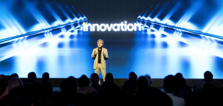 Choi Si-young, President of Samsung Electronics Foundry Division, is delivering the keynote speech at the 'Samsung Foundry Forum 2023' held in Silicon Valley, USA. /
 Photo by Samsung Electronics
Samsung Electronics Unveils '2-nm' Foundry Strategy to Beat TSMC
On the 27th (local time), Samsung Electronics held the 'Samsung Foundry Forum 2023' in Silicon Valley, USA. Under the theme of 'Innovation Beyond Boundaries,' Samsung presented ways to overcome semiconductor limitations in the AI era. Choi Si-young, President of Samsung Electronics' Foundry Business Division, said, "Many customers are developing AI-dedicated semiconductors tailored to their own products and services," adding, "We will lead the AI paradigm shift by innovating gate-all-around (GAA) transistor technology optimized for AI semiconductors."
GAA is a next-generation transistor technology that increases the gate area to enhance data processing speed and power efficiency. It overcomes the limitations of the existing FinFET transistor structure and is considered a game changer in the foundry industry. Samsung Electronics was the first in the industry to introduce GAA technology when it began mass production of the 3 nm process in June last year. Having improved GAA technology over the past year, it expects significant competitiveness in the 2 nm process. Samsung Electronics' DS Division President Kyung Kye-hyun emphasized, "From 2 nm, the industry leader (TSMC) will also adopt GAA," adding, "By then, our technology level will be on par with the industry leader."
Samsung Electronics disclosed detailed plans and technological levels for the 2 nm process, scheduled for mass production in 2025. The company announced that mass production will start with mobile products under SF2, which refers to the 2 nm process. The mass production scope will expand to HPC in 2026 and automotive in 2027. SF2 can improve performance by 12% and power efficiency by 25% compared to SF3 (3 nm second-generation process). The area will be reduced by 5%. The 1.4 nm process is planned for mass production in 2027 as scheduled.
Samsung Electronics is currently mass-producing products based on orders from fabless (semiconductor design) companies using the GAA-based 3 nm first-generation process (SF3E). For SF3, it is in discussions with customers requiring high-performance, low-power technologies for mobile and HPC, with mass production planned for 2024. Some customers are already producing test chips based on SF3. In preparation for SF2 mass production, Samsung plans to secure various high-speed interface design assets (IPs) required by customers by the first half of next year. As the foundry market for processes below 3 nm is expected to grow rapidly, the company plans to focus on customer acquisition in advanced processes.
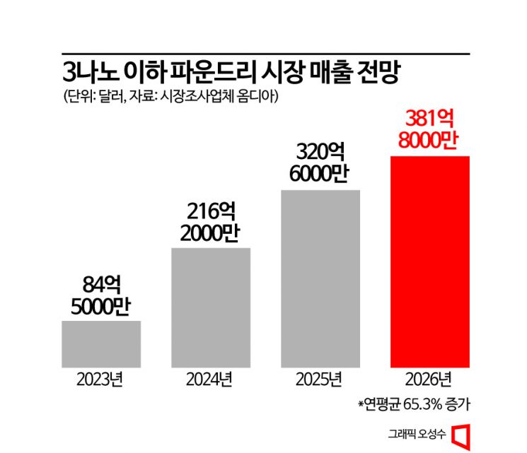
Market research firm Omdia forecasts that the foundry market for processes below 3 nm will grow from $8.55 billion this year to $38.18 billion in 2026, representing an average annual growth rate of 65.3%. The share of processes below 3 nm in total foundry sales is expected to increase from 8% this year to 24.4% in 2026. Expanding to processes below 5 nm could raise the sales share to 41.2% of the total.
Start of 8-inch Power Semiconductor Business... Shell-First and Capacity Expansion Plans
Samsung Electronics is launching new business initiatives to increase revenue in the foundry sector. In 2025, it will start 8-inch gallium nitride (GaN) power semiconductor foundry services for consumer, data center, and automotive applications. Power semiconductors are increasingly used in various devices such as electric vehicles and electronics because they control current direction and power conversion. GaN overcomes the limitations of traditional silicon (Si) semiconductors, maximizing system high-speed switching and power savings.
Samsung Electronics is also developing a 5 nm RF (Radio Frequency) process to secure preemptive technology for 6th generation mobile communication (6G), with mass production planned for the first half of 2025. This process can improve power efficiency by more than 40% and reduce area by 50% compared to the existing 14 nm process. The company also plans to expand the currently mass-produced 8 nm and 14 nm RF processes beyond mobile to various applications including automotive.
Expanding the shell-first strategy to quickly respond to changing market demands is also essential. The shell-first strategy involves proactively building cleanrooms and securing stable production capacity through flexible facility investments linked to future market demand, enabling timely response to customer needs. Samsung Electronics is currently proactively constructing semiconductor cleanrooms in Pyeongtaek, Gyeonggi Province, and Taylor, USA. By 2027, the cleanroom scale is expected to increase 7.3 times compared to 2021.
Expansion of foundry production capacity is also necessary. Samsung plans to begin full-scale mass production of various application products including mobile at Pyeongtaek Line 3 in the second half of the year. The first line of the Taylor plant under construction in the US will be completed in the second half and fully operational by the second half of next year. Additionally, Samsung is developing Yongin as another production base as it transforms into a national industrial complex. Samsung has decided to build five foundry fabs in the system semiconductor cluster to be established in Yongin.
MDI Alliance Launched to Address Packaging Challenges
To meet diverse customer needs, Samsung Electronics collaborates with partners across various fields. The company announced the launch of the 'Multi-Die Integration (MDI) Alliance,' an advanced packaging consortium with global partners in memory, package substrate, and testing sectors, who are part of the 'Samsung Advanced Foundry Ecosystem (SAFE).' The MDI Alliance aims to build an ecosystem for 2.5D and 3D heterogeneous integration (packaging technology that enables semiconductors with different functions to operate as one). It will offer one-stop turnkey services for advanced packaging tailored to different applications.
Gye Jong-wook, Vice President of Samsung Electronics' Foundry Business Division, said, "By collaborating with SAFE partners, we minimize the increased design complexity arising from the adoption of advanced processes and heterogeneous integration technologies," adding, "We will achieve both quantitative and qualitative growth of the SAFE ecosystem through this forum and support customers' innovation and success."
On the 28th (local time), Samsung Electronics will hold the SAFE Forum in Silicon Valley, USA, under the theme 'Accelerating the Speed of Innovation.' The SAFE Forum is an event where Samsung foundry customers and partners gather to share advanced foundry technologies and trends. On the 4th of next month, Samsung will hold the 'Samsung Foundry Forum' and 'SAFE Forum' in Korea. In the second half of the year, Samsung plans to hold foundry forums in Europe and Asia, introducing region-specific customer solutions.
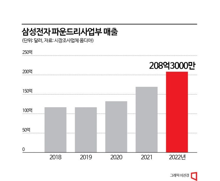
According to statistics from market research firm Counterpoint Research, TSMC recorded a 59% market share in the foundry market in the first quarter, ranking first. Samsung Electronics ranked second with a 13% market share. Another market research firm, TrendForce, reported first-quarter market shares of 60.1% and 12.4%, respectively.
© The Asia Business Daily(www.asiae.co.kr). All rights reserved.
![Clutching a Stolen Dior Bag, Saying "I Hate Being Poor but Real"... The Grotesque Con of a "Human Knockoff" [Slate]](https://cwcontent.asiae.co.kr/asiaresize/183/2026021902243444107_1771435474.jpg)


