Ministry of Science and ICT and Research Institutions Hold Agreement Ceremony on the 1st
Providing On-Site Experience Including Physical Production and Verification of Chip Designs
As Part of Specialized Semiconductor Talent Development
A pathway has opened for semiconductor department undergraduates to gain experience in design, fabrication, and verification so that they can be immediately deployed in the field upon employment.
On the 1st, the Ministry of Science and ICT held a signing ceremony and plaque unveiling at the Electronics and Telecommunications Research Institute (ETRI) in Daejeon to promote the ‘Semiconductor Design Verification Infrastructure Activation Project.’ This marked the official launch of the ‘Design Verification Service for Cultivating Differentiated Semiconductor Design Talent.’ It is one of the follow-up measures to nurture excellent talent in the semiconductor industry, as directed by President Yoon Seok-yeol at the Cabinet meeting in June last year.
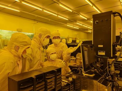
This service provides semiconductor design major undergraduates and graduate students with the opportunity to fabricate and verify the chips they have designed. When a semiconductor chip design fabrication is requested, it is produced and packaged using 500nm CMOS (Complementary Metal-Oxide-Semiconductor) technology at semiconductor fabs operated by ETRI, Seoul National University, and Daegu Gyeongbuk Institute of Science and Technology. Through this, students can directly measure and analyze whether their chips operate as designed, enabling verification.
Until now, semiconductor department undergraduates have had virtually no such opportunities. Graduate students in master’s and doctoral programs have mainly requested chip fabrication from commercial foundries. However, due to high costs, long waiting times, and insufficient feedback, most students found it difficult to access chip fabrication opportunities. Additionally, the PDKs (Process Design Kits) provided by professional foundries contain information that designers need to know and students must learn. However, since PDKs are provided under non-disclosure agreements, they are difficult to offer to undergraduates and are challenging to use in classes.
This program by the Ministry of Science and ICT is the first domestic attempt at a My Chip fabrication service. Utilizing domestic public fabs, it provides free and rapid chip fabrication for undergraduates and graduate students, along with a system for quick feedback on related matters. The Ministry views this as a highly effective educational model for cultivating design talent with practical capabilities.
A pilot service will be offered once starting in the fourth quarter of this year. From next year through 2027, the goal is to provide design verification services more than 6 to 12 times annually. It is expected that over 500 to 1,000 design major students will benefit from chip fabrication each year.
Minister Lee Jong-ho of the Ministry of Science and ICT stated, “In the fierce competition for semiconductor technology supremacy, nurturing semiconductor talent is very important,” and explained, “This was introduced from the perspective that Korea must actively adopt differentiated measures from competing countries to more efficiently secure competitiveness in system semiconductors.”
Meanwhile, students and professors wishing to participate in the service can inquire with the National Nano Infrastructure Council.
© The Asia Business Daily(www.asiae.co.kr). All rights reserved.


