JY Visits Onyang and Cheonan Campuses
Urges Steady Investment in Future Technologies and Talent Acquisition
[Asia Economy Reporter Park Sun-mi] Samsung Electronics Chairman Lee Jae-yong visited the semiconductor packaging lines operating at the Cheonan and Onyang campuses on the 17th to check the next-generation packaging competitiveness and research and development (R&D) capabilities.
Chairman Lee personally inspected the semiconductor production line at the Cheonan campus, where advanced packaging technologies such as HBM (High Bandwidth Memory) and WLP (Wafer Level Package) are applied. During the management meeting held on site, he urged, "Although the situation is difficult, there must be no wavering in nurturing talent and investing in future technologies." Attending the meeting were Kyung Kye-hyun, head of the Semiconductor (DS) Division (President), Lee Jung-bae, head of the Memory Business Division, Choi Si-young, head of the Foundry Business Division, and Park Yong-in, head of the System LSI Business Division.
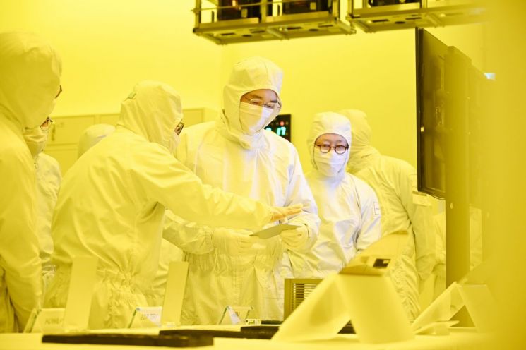
Chairman Lee also held a meeting at the Onyang campus to encourage employees in the packaging technology development department. The employees attending the meeting explained ▲the pride they feel as developers ▲their goals for new technology development ▲and the difficulties they face, and Chairman Lee expressed his gratitude for the dedication and efforts of the executives and staff.
Why Samsung is Focusing on Semiconductor Packaging
The semiconductor packaging process refers to manufacturing semiconductors into forms suitable for electronic devices. It is an essential step that creates pathways for electrical signals and processes the exterior to commercialize the product. High-performance, low-power semiconductor packaging technologies are required in various fields such as artificial intelligence (AI), 5G, and automotive electronics. The importance of advanced packaging technology is increasing as an alternative to overcome the miniaturization limits of semiconductor circuits below 10 nanometers.
Along with Samsung Electronics, global semiconductor companies have recently been focusing on advancing packaging processes. The growing demand for high-performance semiconductors is one reason for the increased investment in packaging. Big tech companies with service platforms like Google and Amazon require customized chips optimized for their services and have also ventured into direct design. For foundry companies entrusted with contract manufacturing, having packaging capabilities that combine different chips to enhance performance presents an opportunity to shake up the market.
Currently, Samsung Electronics operates dedicated packaging production lines at three locations: Onyang and Cheonan in Chungnam Province, and Suzhou in China. The Samsung Electronics DS Division established the 'Advanced Package Team' last year through an organizational restructuring. This is a specialized organization researching packaging technology. It was initially formed as a task force (TF) in June last year, but as the importance of the related field grew, it was promoted to an official team.
The semiconductor packaging market size is growing by 5% annually. Market research firm Gartner predicted that the global packaging market would grow from $48.8 billion (approximately 55 trillion KRW) in 2020 to $51.2 billion (approximately 57 trillion KRW) in 2021, reaching $57.4 billion (approximately 64 trillion KRW) by 2023.
Meanwhile, since his inauguration as chairman, Lee has been visiting regional business sites to thoroughly review business conditions and communicate with local small and medium-sized enterprises (SMEs) as part of his on-site management approach. His first visit after becoming chairman in October last year was to SMEs in the Gwangju region, followed by visits to ▲Busan (SMEs supported by smart factories and Samsung Electro-Mechanics) ▲Daejeon (SSAFY and Samsung Fire & Marine Insurance) ▲Asan (Samsung Display), among others.
© The Asia Business Daily(www.asiae.co.kr). All rights reserved.
![Clutching a Stolen Dior Bag, Saying "I Hate Being Poor but Real"... The Grotesque Con of a "Human Knockoff" [Slate]](https://cwcontent.asiae.co.kr/asiaresize/183/2026021902243444107_1771435474.jpg)


