Thin Film Deposition Process Introduced in December Last Year... "Testing Other Processes"
Early This Year, RCA Analyzed Abnormal Causes; IM Launched with Year-End Process Measurement Results
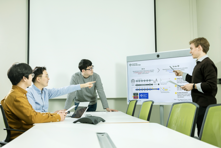 Key figures from SK Hynix and Gauss Labs explaining the development direction of PanoptesVM. Gauss Labs is a U.S.-based industrial artificial intelligence (AI) startup located in Silicon Valley, established with investment funds from SK Hynix. From left to right: Hyunkyung Jung, SK Hynix TL; Donggyun Lim, Gauss Labs Manager; Dohyung Noh, SK Hynix TL; Simon, Gauss Labs employee.
 [Photo by SK Hynix]
[Asia Economy Reporter Moon Chaeseok] SK Hynix announced on the 10th that it has been applying the wafer virtual metrology artificial intelligence (AI) solution 'Panoptes VM' to its mass production fab since last month. Thanks to the new product, process variation was reduced by 21.5% and yield (the ratio of good products among finished products) was improved.
On the same day, SK Hynix revealed that Gauss Labs, an industrial AI startup it invested in, launched the product. It has already been introduced in the mass production fab since last month to enhance productivity.
Panoptes is used in the thin film deposition process, which applies a thin film coating on semiconductor substrates. The thinner and lower refractive index the thin film, the higher the semiconductor quality. The challenge is that 'full inspection' is difficult, but SK Hynix solved this problem by combining AI algorithms with human knowledge.
By using the virtual metrology results of Panoptes VM for process control, it becomes possible to control the process down to individual wafers. This allows for much more precise process control.
Jung Hyunkyung, TL of SK Hynix’s Thin Film Technology Strategy Team, explained, "We collect data such as pressure, temperature, spray distance, gas injection amount, and current inside the chamber during the thin film deposition process, then predict the refractive index and thickness of the film deposited on the wafer through Panoptes VM. This enables us to achieve the effect of full inspection without actually performing full inspection."
Gauss Labs believes that introducing industrial AI will have significant effects in five areas: quality control, production scheduling, equipment repair and maintenance, process and equipment control, and process monitoring. They describe industrial AI as a 'blue ocean' that is less commercialized than consumer AI.
Kim Younghan, CEO of Gauss Labs, stated, "The company is tackling and solving manufacturing site challenges with the best AI technology. We will continue to develop products that will lead innovation in manufacturing, starting with Panoptes VM."
SK Hynix also expressed great satisfaction. Kim Youngsik, Vice President of Manufacturing and Technology at SK Hynix, said, "We are working hard to realize a more intelligent smart factory in cooperation with Gauss Labs. We will continue to secure technological superiority by applying AI technology throughout semiconductor development and production, and the introduction of Panoptes VM is just the beginning."
The two companies are continuing to test industrial AI solutions in processes other than thin film deposition. They plan to collaborate closely to expand products like Panoptes VM to mass production fabs. Lim Dongkyun, Manager at Gauss Labs, hinted, "In addition to Panoptes VM, we plan to launch RCA (Root Cause Analysis solution) early this year and IM (Process Result Metrology solution) by the end of the year."
© The Asia Business Daily(www.asiae.co.kr). All rights reserved.
![Clutching a Stolen Dior Bag, Saying "I Hate Being Poor but Real"... The Grotesque Con of a "Human Knockoff" [Slate]](https://cwcontent.asiae.co.kr/asiaresize/183/2026021902243444107_1771435474.jpg)


