Core Technologies for Maximizing Performance
Packaging Market Expected to Maintain 5% Annual Growth Rate
[Asia Economy Reporter Han Yeju] In the semiconductor ecosystem, which consists of design, foundry, and back-end processes, the importance of "packaging" is growing steadily. As the fine processes that enhance performance with extremely detailed circuits reach their limits, global semiconductor companies are positioning packaging as a product differentiation strategy. Taiwan's TSMC and the US-based Intel have already made investments worth trillions of won. Samsung Electronics, which is betting its life on strengthening its foundry business, is also planning investments to increase packaging production capacity.
According to industry sources on the 20th, global semiconductor companies have recently been focusing on packaging processes.
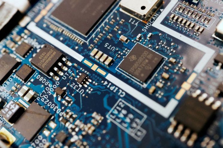
Simply put, packaging means stacking or bundling multiple semiconductors together. In the past, it simply referred to packaging to protect circuits, but now it has emerged as a core technology receiving the most attention. As the limits of semiconductor fine processes restrict the extent of performance improvement, the method of using multiple chips together to maximize performance has become a notable alternative. The fact that each step up to the current 3-nanometer (nm) fine process requires enormous investments worth trillions of won is another reason why packaging technology has become important.
The increasing demand for high-performance semiconductors is also one of the reasons for expanding investments in the packaging field. Big tech companies with service platforms such as Google and Amazon require customized chips optimized for their services and have ventured into direct design. For foundry companies entrusted with manufacturing, those with packaging capabilities that can bundle different chips to enhance performance have the opportunity to shake up the market.
The company showcasing the most advanced packaging technology is undoubtedly Taiwan's TSMC, the number one foundry in the industry. In 2012, TSMC introduced a technology called Chip-on-Wafer-on-Substrate (CoWoS) that integrates four chips. TSMC applies packaging technology from the front-end process stage, where circuits are drawn on the wafer, rather than connecting completed semiconductors. Because semiconductor manufacturing and packaging are done simultaneously, there is no need for a separate substrate. This allows TSMC to make the package 20% thinner than competitors, reduce power loss by 10%, and improve speed by 20%.
In southern Taiwan, TSMC is building a new semiconductor packaging factory. This factory is expected to mainly handle TSMC's flagship 5-nanometer (nm, one billionth of a meter) semiconductors. The new factory will be TSMC's sixth packaging plant in Taiwan. It already operates four factories and is constructing one more in the northern science park. TSMC is also increasing its connections with Japan, which has high packaging technology capabilities. It is building a packaging research and development (R&D) center at the Ibaraki Prefecture Industrial and Technological Research Institute in Japan with an investment of 37 billion yen (approximately 400 billion won). Here, TSMC plans to conduct material research for three-dimensional (3D) integrated circuits (ICs) that stack three semiconductors.

Intel is considered the company investing most actively in the advanced packaging business sector. Intel plans to invest $4.75 billion (about 6 trillion won) in advanced packaging facilities this year, following a $3.5 billion (about 4 trillion won) investment last year. The scale of packaging facility investments by Intel and TSMC is estimated to account for about 60% of the global total.
Samsung Electronics, which is evaluated as having a relatively underdeveloped ecosystem including back-end processing, has recently been focusing on packaging investments. Samsung currently possesses 2.5-dimensional (2.5D) packaging technology that places logic semiconductors and high-bandwidth memory (HBM) on a flat substrate, and 3D (X-Cube) packaging technology that stacks memory (SRAM) on logic integrated circuits (dies) made with the latest extreme ultraviolet (EUV) process. Additionally, Samsung is introducing a 3.5D packaging process that combines customer-customized ultra-high-performance memory with X-Cube packaging.
This year, Samsung Electronics has accelerated the expansion of packaging production capacity by increasing investments in its packaging lines in Cheonan, Chungnam Province. Currently, Samsung operates dedicated packaging production lines in three locations: Onyang and Cheonan in Chungnam, and Suzhou in China. Samsung Electronics' Device Solutions (DS) division recently reorganized to establish the "Advanced Package Team," a specialized organization for researching packaging technology. Initially formed as a task force (TF) in June, it was promoted to a formal team due to the growing importance of the related field. Executive Director Park Cheolmin of the Memory Business Division is in charge.
The semiconductor packaging market is growing about 5% annually and is emerging as a future growth engine for the semiconductor industry. Market research firm Gartner predicted that the global packaging market would grow from $48.8 billion (about 55 trillion won) in 2020 to $51.2 billion (about 57 trillion won) in 2021, reaching $57.4 billion (about 64 trillion won) in 2023. There are also forecasts that packaging technology will receive even more attention as 1-nanometer technology becomes mainstream. An industry insider said, "The development of new technologies such as 3D packaging is essential for manufacturing advanced semiconductor chips below the 2-nanometer process. Fierce competition to secure such technologies is expected over the next five years."
© The Asia Business Daily(www.asiae.co.kr). All rights reserved.


