Exclusive Optical Lens Supply to Dutch ASML
Announcing 48 Billion Investment by 2026
Including Semiconductor and Microscope R&D Facilities
"Continuous Investment Planned for the Future"
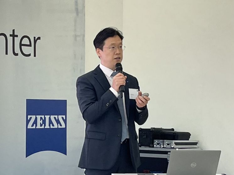 Jung Hyun-seok, CEO of Zeiss Korea, is giving a presentation at the company's Innovation Center in Dongtan, Gyeonggi Province. / Photo by Kim Pyeong-hwa
[Asia Economy Reporter Kim Pyeonghwa] Following a series of global semiconductor equipment companies announcing investment plans in South Korea, German company Zeiss, which exclusively supplies optical lenses to the Dutch firm ASML, has now announced an investment of 48 billion KRW. In this process, Zeiss plans to introduce its first semiconductor research and development (R&D) facility in Asia, located in South Korea, and collaborate with customers to develop customized equipment.
Zeiss Korea revealed these plans on the 23rd at its Innovation Center in Dongtan, Gyeonggi Province. Jung Hyun-seok, CEO of Zeiss Korea, explained the background, saying, "We are investing to develop machines and equipment that precisely check wafer quality at semiconductor R&D facilities tailored to our customers."
Zeiss provides semiconductor manufacturing technology in over 50 countries worldwide, including South Korea. Its business areas also include medical equipment, optical and electronic microscopes, and quality measurement solutions.
Zeiss is especially well-known for supplying optical systems to ASML, the semiconductor industry's "super Eul" (superior subcontractor). ASML equipment is essential in the semiconductor lithography process, and Zeiss exclusively provides the optical lenses for this equipment. Approximately 80% of the world's semiconductors are produced through Zeiss technology. When German President Frank-Walter Steinmeier visited Samsung Electronics' semiconductor hub, the Pyeongtaek campus, earlier this month, he was accompanied by Zeiss representatives.
In Zeiss's overseas business, South Korea ranks fourth in terms of sales importance. Following an investment of 5 billion KRW over the past three years, including the Innovation Center unveiled last August, Zeiss plans to invest 48 billion KRW domestically from next year through 2026. Zeiss Korea intends to introduce R&D facilities in the rapidly growing semiconductor and electron microscope sectors with this investment. The semiconductor R&D facility is targeted to be operational next year.
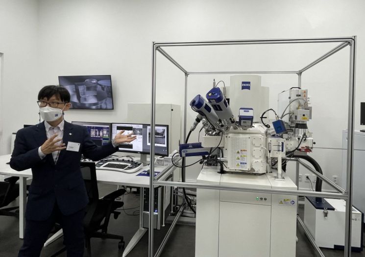 Park Byung-jun, Head of Zeiss Korea, is introducing the Crossbeam 550 device at the Innovation Center. / Photo by Kim Pyeong-hwa
Electron Microscopes Analyzing Semiconductor Components... Photomask Solutions Supporting Lithography Processes
On the same day, Zeiss Korea opened its Innovation Center to the media and introduced various Zeiss equipment. The Innovation Center is a research hub designed to enable core technology development through collaboration while providing various equipment and solution training to domestic customers.
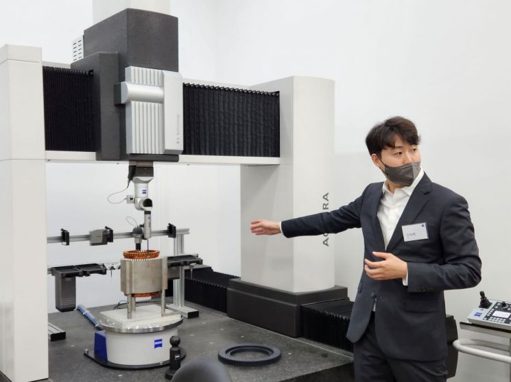
At this location, visitors could see CT equipment such as the 'Metrotom 1500,' electron microscopes like the 'geminiSEM 360,' the 'Crossbeam 550' which combines electron microscopy with focused ion beam (FIB) technology, and the contact-type 3D scanner 'Accura.'
Among these, the geminiSEM 360 and Crossbeam 550 are primarily used in the semiconductor and electronics industries. These products apply Zeiss's optical microscope technology to electron microscopy, allowing for distortion-free observation of semiconductor sample structures and enabling various component analyses. They are capable of observing objects smaller than 1 nanometer (nm; 1 nm = one-billionth of a meter).
Zeiss Korea is also focusing on the semiconductor mask solution (SMS) business domestically. It provides various solutions to improve the quality of photomasks used in lithography equipment to draw fine electronic circuits onto semiconductor wafers.
Lee Jun-seok, Executive Director of Zeiss Korea's Semiconductor Business Division, emphasized, "We support a variety of solutions used in all photomask tasks, including defect repair, correction, inspection, and measurement. We can provide solutions not only for deep ultraviolet (DUV) and extreme ultraviolet (EUV) but also for high NA, the next-generation EUV equipment."
Zeiss Korea has announced its goal to increase domestic sales across various business areas, including semiconductors, batteries, and electric vehicles. CEO Jung stated, "Since multiple businesses are succeeding in the Korean market, we will continue to invest in the industry sector going forward."
© The Asia Business Daily(www.asiae.co.kr). All rights reserved.


