Professor Jaehyun Lee of Ajou University and Professor Seokgyun Son of Mokpo National University Jointly Develop
[Asia Economy Reporter Kim Bong-su] A fundamental technology for developing two-dimensional semiconductor materials that can overcome the physical limitations of conventional silicon semiconductors, which can no longer be further integrated, has been developed.
According to the Korea Research Foundation on the 15th, Professor Jae-Hyun Lee's research team at Ajou University, in collaboration with Professor Seok-Kyun Son at Mokpo National University, succeeded in developing an atomic-spalling method that can control the size and depth of cracks at the atomic level.
Spalling (Atomic-Spalling) refers to the phenomenon where a film spontaneously delaminates due to external stress. Recently, as silicon, the core semiconductor material, has reached its physical size limits in the miniaturization process of semiconductors, various studies have been attempted to discover new semiconductor materials that can replace silicon.
Two-dimensional semiconductor materials, despite being thin materials with a thickness of a single atomic layer in a planar form, maintain high physical properties and are attracting attention as key components to replace silicon and realize next-generation semiconductor devices. A representative method to secure two-dimensional semiconductor materials is the physical exfoliation method, which mechanically separates graphene from graphite using the adhesive force of tape. However, it was impossible to produce due to the inability to control size, yield, and the number of layers.
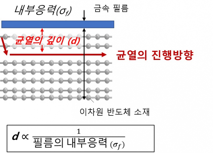
The research team developed an atomic-spalling method that can control the depth and direction of cracks occurring when external stress is applied to two-dimensional semiconductor crystals with a layered structure by utilizing the weak van der Waals force, which is the force attracting electrically neutral molecules at close distances, at the atomic layer thickness level. Unlike conventional physical exfoliation methods that randomly extract materials along cracks, they confirmed that the depth and direction of cracks can be controlled by the interlayer bonding force of the material, the internal stress of the deposited film, and the mechanical properties of the material, allowing selective separation and securing of the material.
In fact, the research team succeeded in securing high-quality two-dimensional semiconductor materials with millimeter-scale large areas and atomic-layer thickness by coating silver in film form on the surface of molybdenum disulfide (MoS2), a representative two-dimensional semiconductor material, and then peeling it off using tape with this atomic-spalling method. Additionally, optical and electrical analyses confirmed that the quality of the materials secured by this method showed no difference from those obtained by conventional physical exfoliation methods. The method was also effective for other two-dimensional semiconductor materials such as molybdenum diselenide (MoSe2) and tungsten diselenide (WSe2), verifying its potential for use with various materials.
The research team stated, “The atomic-spalling method provides a solution to simultaneously address the quality and productivity obstacles considered barriers to the utilization of two-dimensional semiconductor materials,” and added, “It will play an important role in diagnosing and solving the fundamental causes of film delamination problems occurring in electronic devices fabricated with multilayer thin-film* structures.” The results of this study were published online on the 16th of last month in the international materials science journal ‘Matter.’
© The Asia Business Daily(www.asiae.co.kr). All rights reserved.


