UNIST Professor Baek Jongbeom's Team Synthesizes '2D Organic Polymer Structures'
[Asia Economy Yeongnam Reporting Headquarters Reporter Hwang Dooyul] The possibility of applying lightweight and flexible ‘organic semiconductors’ to actual semiconductor devices has opened up.
This is thanks to the synthesis of a new ‘two-dimensional organic semiconductor material’ that compensates for the performance previously inferior to ‘inorganic semiconductors’ like silicon.
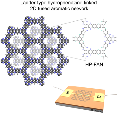
The research team led by Professor Baek Jongbeom of the Department of Energy Chemical Engineering at UNIST announced the synthesis of the ‘HP-FAN (H-P-FAN) two-dimensional organic polymer structure’ through an ‘aromatic cyclization reaction.’
According to the researchers, the new material has a suitable ‘band-gap, high on/off ratio, and charge mobility’ for use as a semiconductor, making it promising for actual semiconductor device applications.
The currently used ‘silicon semiconductor (inorganic semiconductor)’ is hard and heavy, limiting its application in ‘rollable displays’ or ‘wearable electronic devices.’
Graphene, which is light, flexible, strong, and highly conductive, has attracted attention as an alternative semiconductor material, but its band-gap is too small, resulting in a low on/off ratio and difficulty controlling current flow within the semiconductor.
Research on ‘organic semiconductors’ is actively underway as an alternative to overcome the limitations of graphene with these issues.
Organic semiconductors are not only flexible and lightweight like graphene but also have low processing costs and easy tunability of physical properties.
However, organic semiconductors have been difficult to apply as semiconductor devices because electrons and holes move slowly within the material.
When semiconductor devices are made from materials with low charge mobility, electrical signal transmission slows down, causing issues such as color conversion delays in displays.
Professor Baek Jongbeom’s team designed a new HP-FAN structure by reacting two types of chemicals, HAB and DHBQ, to increase the charge mobility of organic semiconductors.
The structure has a two-dimensional aromatic framework with uniform pores and nitrogen atoms added, resulting in an appropriate band-gap, high on/off ratio, and charge mobility.
First author Dr. Noh Hyukjun explained, “We developed a stable and highly crystalline two-dimensional structure and confirmed the semiconductor properties of the material through both experiments and calculations. This research shows excellent performance when applied to actual semiconductor devices and suggests a direction for future material development.”
Research leader Professor Baek Jongbeom stated, “We overcame the chronic problem of ‘low charge mobility’ in two-dimensional polymers used as organic semiconductor materials and the fatal limitation of graphene semiconductors, which is the low on/off ratio. We expect significant progress in developing organic semiconductor device materials that surpass graphene, known as the dream new material.”
The research was conducted in collaboration with Professor Cho Gilwon’s team from the Department of Chemical Engineering at POSTECH, and the paper was published on the 30th in Chem, a sister journal of Cell.
The research was supported by the Ministry of Science and ICT’s Leader Researcher Support Project (Creative Research), the Excellent Science Research Center (SRC), and the U-K Brand Development Project (UNIST).
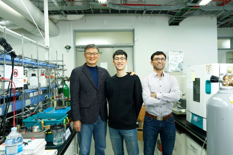 (From left) Professor Jangbeom Baek of UNIST, Dr. Hyeokjun Noh of UNIST, and Dr. Javid Mahmood of UNIST stood in front of the camera.
© The Asia Business Daily(www.asiae.co.kr). All rights reserved.
![Clutching a Stolen Dior Bag, Saying "I Hate Being Poor but Real"... The Grotesque Con of a "Human Knockoff" [Slate]](https://cwcontent.asiae.co.kr/asiaresize/183/2026021902243444107_1771435474.jpg)


