KAIST Develops Method to Improve Efficiency of 3D Lithography Process

[Asia Economy Reporter Kim Bong-su] As Samsung Electronics and Taiwan's TSMC compete to introduce ultra-precise next-generation semiconductor processes such as 3nm and 2nm, a Korean research team has developed a future core technology that could leap ahead.
KAIST announced on the 27th that the research team led by Professors Jeon Seok-woo and Shin Jong-hwa from the Department of Materials Science and Engineering developed a method to efficiently fabricate three-dimensional nano-structures, a core technology for next-generation semiconductor processes, using a single exposure. The exposure process refers to the step of engraving electronic circuits onto silicon wafers using light.
The research team evaluated that compared to the conventional two-dimensional planar exposure method, which fabricates semiconductor structures and wiring layer by layer like building floors, their method provides a basis for manufacturing at much lower cost and with fewer process steps. The research results were published online on the 25th in the international academic journal Science Advances.
The team proposed a methodology that uses an adjoint method-based inverse design algorithm to efficiently find the lattice structure of a phase mask that generates the desired nano hologram with minimal computation. This was applied to existing semiconductor lithography processes, and the team experimentally demonstrated that by exposing a photosensitive material to light only once, the target nano hologram can be formed and materialized, enabling the realization of the desired three-dimensional nano-structure with a single exposure.
With recent advances in lithography and patterning technologies enabling the realization of material shapes at the nanoscale, research on metamaterials and 3D printing that overcome the physical properties of conventional materials is gaining attention. In particular, existing processes used to realize three-dimensional nanomaterials face challenges in simultaneously satisfying freedom of structure, productivity, and precision, prompting various attempts to improve these aspects.
Among various 3D patterning processes, Proximity-field nanoPatterning (PnP) can accurately and productively realize periodic three-dimensional nano-structures with a single exposure. However, until now, the degree of freedom of structures that can be realized using periodic phase mask patterns has been limited. Overcoming this requires calculating the design of a phase mask that implements the desired hologram shape on the photosensitive material.
Previous studies performed such inverse calculations using Genetic Algorithms, but their inefficient computation methods and large computational loads limited practical use. Recently, machine learning has attracted attention, but it requires thousands or more data samples for training, making it still impractical for inverse calculations.
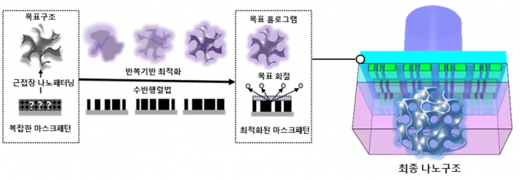
The research team applied an adjoint method-based algorithm, a mathematical methodology, to the optical phenomena of the phase mask pattern interacting with light, successfully calculating and obtaining the desired hologram shape on photosensitive materials efficiently. This algorithm finds the target design expressed in formulas with minimal computational paths and efficiently handles large computational loads using matrix operations. Conventional simple periodic phase mask patterns generated only specific arrays of nanostructures under vertically incident light. In this study, the team succeeded in obtaining new arrays of three-dimensional nanostructures, which were impossible to achieve with existing masks, by using a vertical incidence beam method applicable to semiconductor processes on the phase mask. This research theoretically and experimentally demonstrated that it overcomes the freedom limitations of existing semiconductor exposure processes and enables the realization of more complex nanostructures.
The fabricated three-dimensional nanostructures open possibilities for producing various materials in desired structures by injecting and substituting materials according to the structure using atomic layer deposition methods.
The research team stated, "If this technology is applied to next-generation semiconductor devices such as GAA (Gate All Around) devices or three-dimensional semiconductor integration technologies, it is expected to greatly contribute to strengthening next-generation semiconductor capabilities, which the nation is currently investing significant efforts in." They further explained, "Moreover, this foundational technology will significantly enhance domestic material competitiveness by producing desired nanostructures at low cost and large scale in metamaterial research, which secures new physical properties originating purely from nanostructures rather than atoms or bonds constituting the materials."
© The Asia Business Daily(www.asiae.co.kr). All rights reserved.
![Clutching a Stolen Dior Bag, Saying "I Hate Being Poor but Real"... The Grotesque Con of a "Human Knockoff" [Slate]](https://cwcontent.asiae.co.kr/asiaresize/183/2026021902243444107_1771435474.jpg)


