International Joint Research Team Including Institute for Basic Science Achieves Success in Developing 'Transition Metal Dichalcogenides'
[Asia Economy Reporter Kim Bong-su] Domestic researchers have developed a core technology that will accelerate the commercialization of next-generation semiconductor materials to replace silicon.
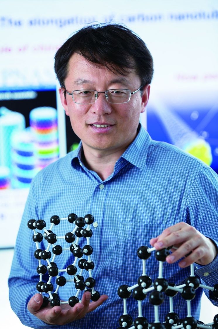
The Institute for Basic Science (IBS) announced on the 16th that the research team led by Feng Ding, Group Leader of the Multidimensional Carbon Materials Research Division (Distinguished Professor, Department of Materials Science and Engineering, Ulsan National Institute of Science and Technology), together with researchers from Peking University and other Chinese institutions, identified the key principles affecting the large-area single crystal growth of transition metal dichalcogenides. Furthermore, the joint research team succeeded in fabricating representative transition metal dichalcogenide materials such as tungsten disulfide (WS2) into wafer-sized single crystals.
As silicon-based semiconductor technology reaches its performance limits, there is a growing demand for new materials that can replace silicon. Transition metal dichalcogenides (TMDs), which possess excellent physical and electrical properties, are attracting attention as next-generation semiconductor materials alongside graphene and black phosphorus. Although research on these materials is being competitively conducted worldwide, mass production has not yet been achieved.
The research team uncovered the core principles that will accelerate the commercialization of transition metal dichalcogenides.
If a semiconductor is compared to a pizza, the wafer is the dough. Just as the state of the dough is crucial to the taste of the pizza, the quality of the wafer determines the performance of the semiconductor. The growth method mainly used to produce high-performance wafers is called ‘epitaxial growth.’ The key technology of epitaxial growth is to ensure that all small single crystals grown on the substrate are uniformly aligned. However, in the case of transition metal dichalcogenides, substrate selection is challenging because they consist of two elements and their structural symmetry points are located at the edges rather than the center.
In this study, based on theoretical calculations, the research team proposed a principle for selecting customized substrates with unique symmetrical structures for transition metal dichalcogenides and named this method the ‘double-bond induced epitaxial growth method.’ For example, in the case of tungsten disulfide (WS2), two opposite preferred directions exist during synthesis, but when an insulating sapphire substrate is used, all WS2 grown at the step edges on the substrate align in a single direction. The crystal grains at the step edges gradually grow to form a large-area single crystal of the same size as the substrate.
Researcher Ting Cheng explained, “Based on the ‘double-bond induced epitaxial growth method,’ selecting an appropriate substrate theoretically makes it possible to grow all two-dimensional materials into large-area single crystals.”
Using the same method, the research team also succeeded in producing large-area 2-inch wafer-sized transition metal dichalcogenides such as molybdenum disulfide (MoS2), tungsten diselenide (WSe2), and molybdenum diselenide (MoSe2). This achievement marks a breakthrough that can significantly accelerate the practical application of new semiconductor materials to succeed silicon.
Group Leader Feng Ding stated, “Following graphene and hexagonal boron nitride (hBN), which are ‘predecessors’ of two-dimensional materials, transition metal dichalcogenides can now also be fabricated as wafer-sized single crystals. This is a monumental study that will be recorded in the history of two-dimensional materials and will drive advancements in high-performance electronic and optical devices.”
The research results were published on the 16th at 1 a.m. (Korean time) in the international nanoscience journal Nature Nanotechnology (IF 39.213).
© The Asia Business Daily(www.asiae.co.kr). All rights reserved.


