Samsung Electronics to Mass-Produce World's First GAA-Based 3nm Chip Next Year
Global Foundry Attempts Paradigm Shift in Process Technology
TSMC Plans GAA Adoption in 2023, Intel in 2024
Transistor Structure Innovation Ensures Performance and Efficiency
[Asia Economy Reporter Suyeon Woo] As the power struggle among South Korea, Taiwan, and the United States intensifies in the global foundry market, securing ‘GAA (Gate All Around)’ technology is emerging as a new competitive field. While the industry has focused on the ‘nano competition’ to reduce semiconductor line widths, it is now concentrating on developing new-concept semiconductors that enhance performance and efficiency by securing structural innovation technology for semiconductor devices.
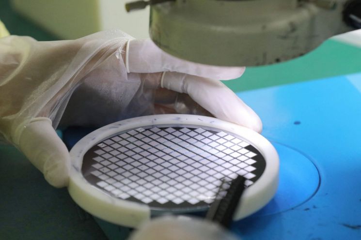
According to the industry on the 3rd, Samsung Electronics plans to mass-produce its first-generation 3nm products based on GAA technology starting next year, and in 2023, it will apply GAA technology to the second-generation 3nm process. GAA refers to a new structural process technology that improves the performance and efficiency of transistors, which act as current control switches in semiconductors.
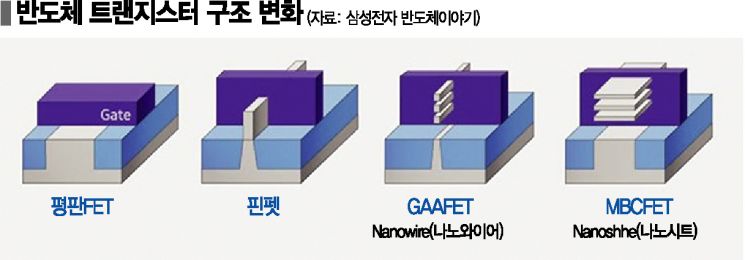
To reduce the size of transistors while maintaining precise control, it is advantageous for the internal structures to have a larger contact area. For this reason, the structure evolved from the initial planar form to the currently widely used three-dimensional FinFET structure, and now GAA, which utilizes thin and long wire-shaped channels, is gaining attention.
GAA itself is a revolutionary technology that is called an industrial revolution in the semiconductor industry. Samsung has taken a step further by developing its proprietary ‘MBCFET’ technology, which applies ‘nanosheets’ shaped like thin, long sheets similar to paper to improve efficiency. Applying this technology can increase performance by 35% and reduce power consumption by 50% compared to existing 7nm FinFET transistors.
Currently, in the nano competition to reduce semiconductor line widths, TSMC is considered the industry leader. Recently, TSMC began testing 3nm products with customers such as Apple and Intel and is preparing for mass production in the second half of next year. Samsung also aims to introduce the 3nm process next year but is still at the tape-out stage (the phase of handing over design blueprints to manufacturers after process development). Intel is far behind at the 7nm level.
However, the story changes when the competition criterion shifts to ‘GAA adoption.’ Samsung plans to be the first to adopt GAA starting with the 3nm process next year, followed by TSMC, which plans to introduce GAA from the 2nm process in 2023. Intel has also declared it will apply its own GAA technology, ‘RibbonFET,’ to the 2nm process in 2024, entering the GAA competition.
From Samsung’s perspective, the title of ‘world’s first 3nm mass production’ may be taken by TSMC due to scheduling, but Samsung can lead the world’s first GAA adoption and aim for a paradigm shift in foundry processes. Samsung Electronics’ strategy is to change the global foundry process competition landscape through GAA.
Hwang Minseong, a researcher at Samsung Securities, said, "Samsung will regain leadership in process development compared to TSMC starting with the GAA process applied from 3nm," adding, "Despite adverse factors such as the suspension of operations at the Austin plant, Samsung’s foundry sales are growing at about 20% this year, and sustained growth based on next-generation GAA processes is expected in the future."
© The Asia Business Daily(www.asiae.co.kr). All rights reserved.


