Development of Material Growth Method Stacking Up to 9 Different Atomic Layers
Securing Core Technology for Quantum Computing
Enabling Use in Ultra-Small, Low-Power Electronic Devices
[Asia Economy Reporter Kim Bong-su] Korean researchers have developed a material growth method that stacks different atomic layers one by one for the first time in the world, signaling a breakthrough in securing core technology for quantum computing.
The Institute for Basic Science (IBS) announced on the 19th that the research team led by Deputy Director Moonho Cho of the Atomic Control Low-Dimensional Electronic Systems Research Group (POSTECH professor) developed a material growth method that stacks different atomic layer semiconductors, realizing a new material with an atomic-layer-thick two-dimensional semiconductor superlattice structure for the first time worldwide. The team explained, "This presents a new quantum information semiconductor platform and is expected to accelerate the securing of core technology for quantum computing."
The technology to create semiconductor superlattice structures (periodic layers of two or more materials) through a two-layer single junction has already been developed. By artificially controlling the periodic arrangement of different atoms, it is widely used in high-performance semiconductors, lasers, and display industries. A representative example is light-emitting diode (LED) technology, which was completed through a superlattice structure composed of repeated layers of chemical substances such as gallium nitride at the scale of several nanometers.
However, existing superlattice structure materials were difficult to apply to two-dimensional semiconductors due to strong covalent bonding. Among various semiconductors, two-dimensional semiconductors with almost no thickness are considered key materials for realizing ultra-small and low-power electronic devices. Until now, technology to stack and control two or more types of two-dimensional semiconductors at the atomic level through weak interlayer interactions had not been realized.
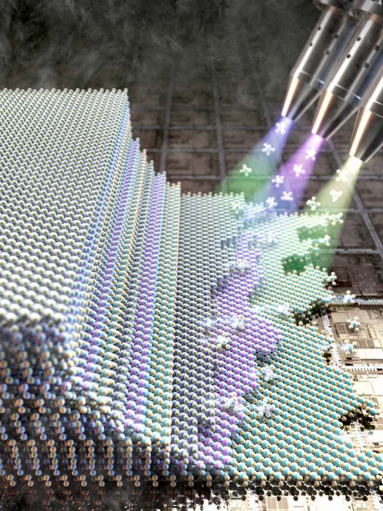
The research team continuously applied junction technology to realize, for the first time, a semiconductor superlattice structure where different atomic layer semiconductors are repeated up to nine layers. Using metal-organic chemical vapor deposition, the researchers controlled the types and order of two-dimensional semiconductors such as molybdenum disulfide (MoS2), tungsten disulfide (WS2), and tungsten diselenide (WSe2) to develop an artificial semiconductor material with a new structure.
Using the two-dimensional semiconductor superlattice growth method developed by the research team, artificial control of atomic species and periodicity at the atomic layer level is possible. This allows for the free design of new artificial materials, which can lead to semiconductor technologies with various electronic structures.
The team also confirmed the storage of a new degree of freedom of charge called valley. The valley can be used as a medium for quantum information in two-dimensional semiconductor superlattice structures. All single-layer two-dimensional semiconductor materials possess valley degrees of freedom, which are expected to store quantum information capable of representing two or more values simultaneously or enabling parallel computation. The research team confirmed that the number of superlattice repetitions is proportional to the stored quantum information and that this information remains intact. Therefore, the new semiconductor superlattice is expected to be utilized as a quantum semiconductor platform capable of quantum information processing.
Deputy Director Moonho Cho said, "The two-dimensional semiconductor superlattice structure will present a new direction for modern electronic or optoelectronic semiconductor technology," adding, "It could become one of the core technologies in the field of next-generation quantum computing devices."
This research was published on the 16th in the world-renowned journal Nature Nanotechnology (IF=39.213).
© The Asia Business Daily(www.asiae.co.kr). All rights reserved.


