First Introduction of Extreme Ultraviolet (EUV) Microlithography Process
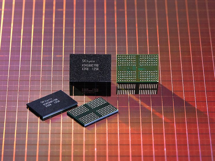
[Asia Economy Reporters Heungsun Kim and Hyunjin Jung] SK Hynix has begun mass production of 10-nanometer-class 4th generation (1a) mobile DRAM, applying extreme ultraviolet (EUV) fine process technology for the first time.
SK Hynix announced on the 12th that it started mass production of 8Gbit LPDDR4 using the next-generation 10-nanometer-class 4th generation (1a) fine process earlier this month. DDR is the standard name for DRAM defined by the JEDEC (Joint Electron Device Engineering Council). The generations have evolved from DDR1 to DDR4. LPDDR4, with the prefix 'LP', refers to low-power memory developed for mobile devices such as smartphones. Unlike the previous LPDDR3 which used voltages of 1.2 to 1.8V, LPDDR4 uses 1.1 to 1.8V to reduce power consumption.
Increased Productivity and Price Competitiveness
Supply to Smartphone Manufacturers in the Second Half
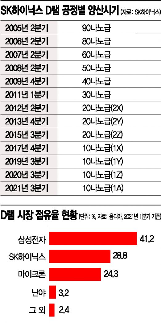
The semiconductor industry assigns alphabetic symbols to each generation starting from 10-nanometer-class DRAM. 1a is the 4th generation technology following 1x (1st generation), 1y (2nd generation), and 1z (3rd generation). SK Hynix has started mass production of new products by applying EUV process technology for the first time among the DRAM it produces.
To manufacture semiconductors, circuits that serve as blueprints must first be drawn on wafers (semiconductor discs). Traditionally, circuits were drawn using argon fluoride (ArF) processes, but there is a growing preference for EUV lithography equipment, which uses shorter wavelengths than ArF light, for more precise work.
An industry insider explained, "Using EUV equipment is like using a thinner and more precise pen to make the lines finer. This allows for more precise circuit drawing," adding, "The process of repeatedly engraving circuits is shortened, and product productivity improves, which benefits both manufacturers and customers in gaining price competitiveness."
Previously, SK Hynix partially introduced EUV during the production of 1y (2nd generation) products to verify stability. According to SK Hynix, 1a DRAM applying EUV process technology yields about 25% more products per wafer compared to the same specifications of the previous 3rd generation technology.
The new product also stably achieves the highest speed (4266Mbps) of the LPDDR4 mobile DRAM standard while reducing power consumption by about 20% compared to existing products. By enhancing its low-power strengths, the company emphasized that this model aligns with ESG (Environmental, Social, and Governance) management by reducing carbon emissions.
"Expanding the Proportion of EUV Process Applied DRAM"
Expectations to Strengthen Market Dominance
SK Hynix plans to supply the new mobile DRAM product with 1a technology to smartphone manufacturers starting in the second half of this year. It also plans to apply 1a technology to next-generation DDR5 DRAM, which was first launched worldwide in October last year, starting early next year. Going forward, the company intends to produce all 1a DRAM products using EUV.
To increase the proportion of products incorporating advanced fine processes, related investments are also being expanded. EUV lithography equipment is exclusively supplied by the Dutch semiconductor equipment company ASML and is highly advanced, with a price approaching 200 billion KRW per unit. Earlier this year, SK Hynix signed a contract with ASML to invest about 4.8 trillion KRW over the next five years to additionally introduce EUV lithography equipment.
In February, SK Hynix completed the 'M16 Fab (production plant)' at its headquarters in Icheon, Gyeonggi Province, which is noted as the world's largest new memory semiconductor production line. Along with the 'M14 Fab' established in 2015, it is expected to be used as a base for producing products applying next-generation technology.
According to market research firm Omdia, as of the first quarter of this year, SK Hynix holds the world's second-largest market share in DRAM at 28.8%. The company expects that mass production of 1a DRAM will strengthen its market dominance and enhance its influence in memory semiconductor supply and demand.
Cho Young-man, Vice President of SK Hynix and head of the 1a DRAM task force (TF), said, "1a DRAM is a product with improved productivity and cost competitiveness, allowing for high profitability," adding, "By fully applying EUV to mass production, we expect to solidify our position as a leading company in cutting-edge technology."
© The Asia Business Daily(www.asiae.co.kr). All rights reserved.
![Clutching a Stolen Dior Bag, Saying "I Hate Being Poor but Real"... The Grotesque Con of a "Human Knockoff" [Slate]](https://cwcontent.asiae.co.kr/asiaresize/183/2026021902243444107_1771435474.jpg)


