K-Semiconductor Strategy
Over 510 Trillion Won Investment by 2030... Establishing the World's Largest and Most Advanced Semiconductor Supply Chain
40-50% Tax Credit for R&D · 10-20% for Facility Investment
Training a Total of 36,000 Semiconductor Workforce Over 10 Years
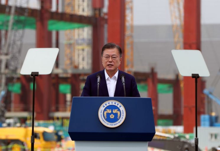 President Moon Jae-in is speaking at the 'K-Semiconductor Strategy Report' held on the outdoor stage set up at the Samsung Electronics Pyeongtaek Complex Line 3 construction site in Pyeongtaek-si, Gyeonggi-do, on the afternoon of the 13th. [Image source=Yonhap News]
[Sejong=Asia Economy Reporter Joo Sang-don] The government has decided to establish a 'Special Fund for Semiconductor Facility Investment' worth over 1 trillion won to support the expansion of 8-inch foundries and investments in materials, parts, equipment, and advanced packaging facilities to expand semiconductor infrastructure. Additionally, through the introduction of core strategic technologies, this year’s research and development (R&D) expenses will receive up to a 50% tax credit, and facility investment expenses up to 16%. Including these measures, the goal is to invest more than 510 trillion won by 2030 to complete the world's largest and most advanced semiconductor supply chain.
On the 13th, the government announced the 'K-Semiconductor Strategy' containing these details at Samsung Electronics’ Pyeongtaek Campus.
◆ Establishment of 'Special Fund for Facility Investment' worth 1 trillion won + α = The government will first establish a special fund for semiconductor facility investment worth '1 trillion won + α' to support the expansion of 8-inch foundries and investments in materials, parts, equipment, and advanced packaging facilities. The interest rate will be reduced by 1 percentage point, with a 5-year grace period and 15-year installment repayment applied. The government plans to maximize the scale of support such as business competitiveness enhancement funds and actively support various financial programs.
Furthermore, to secure core technologies and promote the expansion of mass production facilities, core strategic technologies will be introduced, strengthening tax credits for investments made from the second half of this year through 2024. For R&D investment, large and medium-sized enterprises will receive a 30-40% deduction, and small and medium-sized enterprises (SMEs) will receive 40-50%. For facility investment, large enterprises will receive a 6% credit, medium-sized enterprises 8%, and SMEs 16%, with an additional 4% credit on the increased amount regardless of company size.
Regulatory easing will also be pursued. Regulations related to semiconductor manufacturing facilities such as chemical substance handling facilities, high-pressure gases, greenhouse gases, and radio wave application equipment will be rationalized by introducing a fast-track for rapid approval of chemical substance handling facilities. Additionally, when building power infrastructure for semiconductor manufacturing facilities related to core strategic technologies, the government and Korea Electric Power Corporation will jointly share up to 50% of the costs.
The government expects that through this initial investment, total private investment will exceed 40 trillion won this year and surpass 510 trillion won by 2030.
◆ Establishment of the 'K-Semiconductor Belt' to Stabilize the Semiconductor Supply Chain = The government plans to establish the K-Semiconductor Belt connecting Yongin as the center with Pangyo, Giheung~Hwaseong~Pyeongtaek~Onyang, and Icheon~Cheongju. In manufacturing, the focus will be on maintaining the memory super-gap through expansion and advancement of advanced memory manufacturing facilities and promoting new and expanded foundries to stabilize the domestic semiconductor supply chain. A specialized materials, parts, and equipment cluster will be created by linking and integrating large-scale semiconductor fabless (design companies) and materials, parts, and equipment companies in the Yongin semiconductor cluster.
To complement the domestic semiconductor supply chain, foreign-invested companies will be actively attracted in areas where short-term technological catch-up is difficult domestically, such as extreme ultraviolet (EUV) lithography, advanced etching, and materials. First, the government will attract ASML’s training center, which exclusively supplies advanced EUV equipment, and promote doubling the production capacity of Lam Research.
Alongside this, an advanced packaging platform will be established by creating an advanced packaging production base for implementing various functions on a single chip and investing in five next-generation packaging technologies. Furthermore, Pangyo will be developed into a Korean-style fabless valley through the establishment of a system semiconductor design support center, an artificial intelligence (AI) semiconductor innovation design center, and a next-generation semiconductor complex.
◆ Training 36,000 Semiconductor Industry Workforce Over 10 Years = The government will also strengthen workforce training and management. The goal is to train 36,000 semiconductor industry workers over 10 years (2022-2031) through expanding university quotas and providing full-cycle support from bachelor's to master's and doctoral degrees, as well as practical training. To this end, the semiconductor quota will be increased by 150 through adjusting university department quotas and activating minors and double majors. To cultivate practical bachelor-level talent, new contract departments (5 universities) linked with semiconductor equipment companies will be established with major tracks.
Additionally, through the establishment and expansion of industry-academia-linked education programs, excellent master's and doctoral researchers will be nurtured, and practical infrastructure related to semiconductor design and processes will be expanded to provide specialized practical semiconductor education for current workers and job seekers.
To prevent the outflow of core personnel, a compensation system for long-term employees and retirees will also be created. New 'Semiconductor Masters' will be designated, job invention compensation will be enhanced, semiconductor medals and orders will be upgraded, and retirees will be increasingly hired as patent examiners in advanced technology fields and special R&D professors.
Minister of Trade, Industry and Energy Moon Seung-wook said, "In response to the large-scale private investment exceeding 510 trillion won, the government will spare no effort in comprehensive support such as increasing the investment tax credit more than fivefold and establishing a special fund for semiconductor facility investment worth 1 trillion won." He added, "If the K-Semiconductor Strategy is implemented smoothly, exports are expected to increase from $99.2 billion in 2020 to $200 billion in 2030, and employment is expected to grow to a total of 270,000."
© The Asia Business Daily(www.asiae.co.kr). All rights reserved.
![Clutching a Stolen Dior Bag, Saying "I Hate Being Poor but Real"... The Grotesque Con of a "Human Knockoff" [Slate]](https://cwcontent.asiae.co.kr/asiaresize/183/2026021902243444107_1771435474.jpg)


