KAIST Professor Jang Minseok's Team and International Collaborative Researchers Achieve Results Using Graphene Plasmons
Published in Nature Communications on February 19
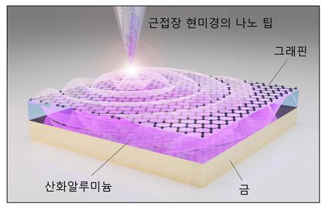 Conceptual diagram of a laser irradiated on a nano tip exciting acoustic plasmons between gold and graphene. Provided by Korea Advanced Institute of Science and Technology (KAIST)
[Asia Economy Reporter Kim Bong-su] An international joint research team led by Korean researchers has obtained the world's first image of mid-infrared waves condensed over a thousand times in a graphene nanolayer structure, observing the behavior of electromagnetic waves in the ultrasmall scale.
According to the Korea Advanced Institute of Science and Technology (KAIST) on the 2nd, an international joint research team led by Professor Minseok Jang of the Department of Electrical Engineering at KAIST recently achieved these results using 'graphene plasmons' highly condensed in waveguides only a few nanometers in size. The study was published on the 19th of last month in the international academic journal Nature Communications.
Graphene plasmons refer to the phenomenon where free electrons in the nanomaterial graphene collectively oscillate by coupling with electromagnetic waves. Recently, it was discovered that these plasmons can confine light within an extremely thin dielectric layer between graphene and a metal plate, creating new modes.
In such a graphene-dielectric-metal plate structure, charges in graphene induce image charges on the metal plate, and when graphene's electrons oscillate due to the electric field of light, the image charges on the metal also oscillate accordingly. This new form of collective electron oscillation mode in the graphene-dielectric-metal plate structure is called the 'acoustic' graphene plasmon (AGP).
However, because AGPs condense optical waves into structures only a few nanometers thick, the electromagnetic field intensity leaking outside is very weak. Therefore, until now, their existence could not be revealed by direct optical detection methods, and only indirect methods such as far-field infrared spectroscopy or photocurrent mapping could demonstrate the presence of AGPs.
To overcome these limitations, the international joint research team proposed new experimental techniques and nanofabrication methodologies. Professor Minseok Jang and postdoctoral researcher Sergey Menabde of KAIST's Department of Electrical Engineering used a highly sensitive scattering-type scanning near-field optical microscope (s-SNOM) to directly detect AGPs oscillating along nanometer-scale waveguides for the first time in the world, visualizing the phenomenon of mid-infrared waves condensed over a thousand times. The nanostructures were fabricated by Professor Sanghyun Oh's team at the Department of Electrical and Computer Engineering, University of Minnesota, USA, and the graphene was synthesized by the team led by Research Director Younghee Lee of the IBS Center for Integrated Nanostructure Physics (CINAP) at Sungkyunkwan University.
The research team detected AGPs even though most of the AGP energy was concentrated in the dielectric layer beneath the graphene. This was possible because the highly flat nanowaveguides created by Professor Sanghyun Oh and Dr. Inho Lee, and the high-purity, large-area graphene synthesized by CINAP, provided an environment where plasmons could propagate over longer distances.
Electromagnetic waves in the mid-infrared region have frequencies matching the vibrational frequencies of various molecules, playing a significant role in studying their chemical and physical properties. For example, many important organic molecules can be detected by mid-infrared absorption spectroscopy. However, the interaction between a single molecule and light is very weak, requiring a large number of molecules for successful detection. AGPs can greatly enhance the interaction between molecules and light through ultra-highly condensed electromagnetic fields, ultimately enabling single-molecule detection technology that works with just one molecule.
Moreover, typical graphene plasmon-based optical devices have difficulty achieving high performance due to large energy absorption in graphene. In contrast, since most of the AGP electromagnetic field exists in the dielectric layer rather than graphene, it is less sensitive to energy loss in graphene, making it advantageous for implementing high-performance devices. This research result offers hope that AGPs can replace other graphene-based metasurfaces, optical switches, and various photocurrent devices operating in the mid-infrared region.
Professor Minseok Jang said, "Through this research, we were able to observe the ultra-highly condensed electromagnetic field of acoustic graphene plasmons via near-field measurements." He added, "We expect that research using acoustic graphene plasmons will become active in other situations requiring strong material-light interactions."
© The Asia Business Daily(www.asiae.co.kr). All rights reserved.


