 Samsung Electronics announced on the 13th that it has successfully produced a test chip applying the industry's first 7-nanometer extreme ultraviolet (EUV) system semiconductor with the three-dimensional stacking package technology called 'X-Cube'.
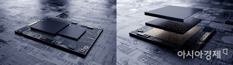
The left side shows the planar design of the existing system semiconductor, and the right side shows the system semiconductor design applying Samsung Electronics' three-dimensional stacking technology 'X-Cube'.
[Asia Economy Reporter Changhwan Lee] Samsung Electronics has succeeded in producing semiconductors using the world's first 3D stacked package technology in the foundry (semiconductor contract manufacturing) sector.
This is a core technology that can enhance the competitiveness of high-performance system semiconductors. Based on this, Samsung Electronics has set a strategy to expand its technological lead over competitors and achieve the number one position in system semiconductors by 2030.
On the 13th, Samsung Electronics announced that it succeeded in producing test chips applying the 3D stacked package technology called 'X-Cube' to 7-nanometer extreme ultraviolet (EUV) system semiconductors. X-Cube is a technology that stacks chips in wafer form, after all processes are completed, thinly on top of each other to create a single semiconductor.
System semiconductors are generally designed by placing the logic part, which performs roles such as central processing units (CPU) and graphics processing units (GPU), and the SRAM part, which acts as cache memory, side by side on a single chip in a planar layout. Cache memory is a temporary storage space that stores frequently performed tasks or operations, enabling faster processing without passing through the main memory, DRAM.
The X-Cube technology designs and produces logic and SRAM separately and stacks them vertically, allowing for a reduction in the overall chip area while equipping high-capacity memory solutions, thereby increasing the design freedom for customers.
While competitors such as TSMC have only disclosed the theory of 3D stacking technology, they have not yet implemented it practically. This time, Samsung Electronics succeeded in mass-producing semiconductors applying this technology for the first time in the world.
Additionally, applying X-Cube can dramatically improve the data processing speed of system semiconductors and increase power efficiency through Through Silicon Via (TSV) technology. TSV is a packaging technology that connects the top and bottom chips with electrodes by drilling tiny holes in the chip instead of using wires, significantly improving speed and power consumption.
Samsung Electronics has previously mass-produced memory (DRAM) and system semiconductors (image sensors) applying TSV technology, a core element of 3D stacking technology. Furthermore, this technology allows the data communication channels between the upper and lower chips to be freely expanded according to customer design, and minimizes signal transmission paths to maximize data processing speed.
This technology is expected to be utilized as a core technology to enhance competitiveness in fields requiring high-performance system semiconductors such as supercomputers, artificial intelligence (AI), and 5G communications, as well as in smartphones and wearable devices.
In particular, global fabless customers can immediately start developing 5- and 7-nanometer process chips based on EUV technology by utilizing Samsung Electronics' X-Cube design methodology and design flow.
Since they can use Samsung Electronics' already verified mass production infrastructure, the company explains that they can quickly identify development errors and shorten chip development time.
Kang Moon-soo, Executive Vice President of the Market Strategy Team at Samsung Electronics' Foundry Business Division, said, "We have stably implemented TSV technology even in advanced processes where EUV equipment is applied," and added, "Samsung Electronics will continue to innovate technologies to overcome the performance limits of semiconductors."
© The Asia Business Daily(www.asiae.co.kr). All rights reserved.
![Clutching a Stolen Dior Bag, Saying "I Hate Being Poor but Real"... The Grotesque Con of a "Human Knockoff" [Slate]](https://cwcontent.asiae.co.kr/asiaresize/183/2026021902243444107_1771435474.jpg)


