[Asia Economy Reporter Junho Hwang] A domestic research team has developed technology that can store information directly at the atomic level. This technology reduces the size limit of memory devices, which has been stuck at 10 nanometers (one billionth of a meter, nm), down to about 0.5 nm, or when configured as the smallest existing memory device size, can increase storage capacity by more than 1000 times. It is expected to open a new chapter in flexible devices and ultra-high integration and ultra-low power artificial intelligence semiconductors.
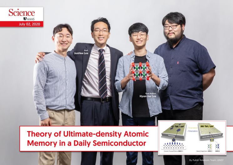
The research team led by Professor Junhee Lee of the Department of Energy and Chemical Engineering at Ulsan National Institute of Science and Technology (UNIST) developed semiconductor technology that can store information at the atomic level using hafnium oxide (HfO2), and announced that the related research results were published on the 3rd (local time) in the international academic journal Science.
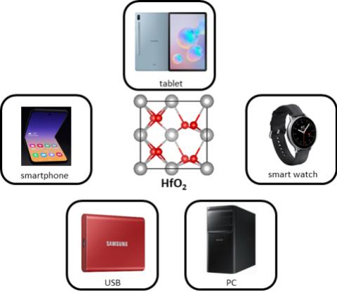
Development of 'Atomic Semiconductor' Using Hafnium Oxide
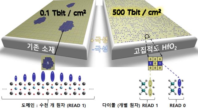 When storing 1 bit, instead of using domains (left) consisting of thousands of atomic groups, individual atoms are directly controlled for storage. Accordingly, thousands of bits can be integrated and used within the area of a conventional 1-bit memory. If advanced microelectrode technology follows, it will be possible to implement atomic memory inside semiconductors with a final integration density corresponding to 500 Tb/cm².
It is unusual for a purely theoretical paper to be published in Science. Science verified the research results through a long review process lasting nine months and decided to publish Professor Lee’s paper with praise. It appears that the potential to become a core technology surpassing the current limits of semiconductors was a significant factor.
The research team proved that information can be stored by controlling atoms. They discovered a new physical phenomenon in the semiconductor hafnium oxide (HfO2) where applying a specific voltage completely eliminates the interaction that tightly binds atoms like a spring. Through this, they confirmed that the positions of atoms (groups of four oxygen atoms) inside the solid semiconductor can be controlled by voltage.
They demonstrated that this method of using voltage as a natural shielding layer to change the positions of groups of four oxygen atoms inside the semiconductor can be utilized as a memory device to store information. Previously, it was believed impossible to individually control each atom due to strong elastic interactions between atoms, but this research broke that fixed notion.
Can Reduce Size or Increase Capacity by More Than 1000 Times
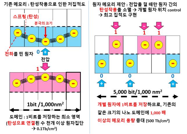 Existing memory (left) requires thousands of atomic clusters (domains) tens of nanometers in size to move simultaneously through interatomic spring-like interactions to store one bit. However, in the newly developed atomic memory using single atoms (right), when a specific voltage is applied, the elastic interactions between atoms completely disappear, allowing individual bit storage in separate atomic groups (clusters of four oxygen atoms).
The research team expects this study to contribute to breaking the size limits of memory devices or developing memory with 1000 times increased capacity at the current size.
By applying this technology, the unit cell size limit of memory devices, which has been stuck at about 10 nm, can be instantly reduced to 0.5 nm (a bundle of four oxygen atoms). Alternatively, the current planar memory integration of 0.1 Tbit/㎠ can be increased by more than 1000 times, enabling ultra-high integration of 500 Tbit/㎠. Integration density is a unit indicating how many bits can be stored per square centimeter.
In particular, the semiconductor industry has faced limits due to scaling phenomena where all semiconductors lose storage capability when the process goes below several tens of nanometers. Currently, ferroelectric memory (FeRAM) processes are about 20 nm, and flash memory processes cannot shrink below a 10 nm line width.
Professor Junhee Lee said, "This theory, which can store information in individual atoms, could become an important foundation for securing global competitiveness in the field of ultra-high integration semiconductors in the future. Unless atoms are split, this technology is likely to be the last integrated storage technology in the current semiconductor industry." He added, "Since the publication of the paper inevitably triggers competition with industries in other countries, rapid demonstration and commercialization require investments from the government and companies."
© The Asia Business Daily(www.asiae.co.kr). All rights reserved.


