[Asia Economy Reporters Hyewon Kim and Dongwoo Lee] Samsung Electronics' decision to embark on a trillion-won 'relay investment' to expand its NAND flash line following the establishment of foundry (semiconductor contract manufacturing) facilities at its new semiconductor plant (P2) in Pyeongtaek, Gyeonggi Province, is part of a strategy to expand its global 'super-gap' with unrivaled manufacturing and technological competitiveness. The 7th generation V-NAND, which Samsung plans to mass-produce as its main product from the second half of next year on the expanded line, is the industry's first product with more than 160 layers of circuit stacking. Successful commercialization will mark an important milestone that can further widen the technological gap with competitors.
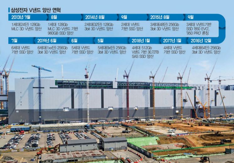
On the 1st, Samsung Electronics announced plans to invest about 9 trillion won to expand the NAND flash line at the P2 campus in Pyeongtaek, establishing two major hubs for next-generation NAND processes: Pyeongtaek domestically and Xi'an, China, overseas. Samsung aims to maintain its global No. 1 position in NAND flash, which it has held for 18 years since 2002, based on its next-generation memory semiconductor manufacturing bases. After being the first in the industry to mass-produce 6th generation V-NAND products in July last year, Samsung is actively developing next-generation ultra-high stacking NAND flash memory with more than 160 layers, surpassing the previous maximum of 128 layers. NAND flash, which stores data, increases storage capacity by increasing the number of NAND cells (data storage spaces) within the same size. The more layers stacked, the greater the capacity and the wider the range of applications.
Industry insiders refer to this as '3D NAND flash,' but Samsung uniquely calls it 'V-NAND flash.' The maximum stacking number of currently commercialized NAND flash memory is 128 layers. Among overseas competitors, China's Yangtze Memory Technologies Co. (YMTC) has announced plans for mass production within the year, closely chasing Samsung Electronics and SK Hynix. Park Jae-geun, chairman of the Korea Semiconductor Display Technology Society, said, "This expansion investment in the Pyeongtaek P2 line appears to be preparation for markets outside China," adding, "Although Samsung's semiconductor production plant in Xi'an, China, mainly serves Chinese demand, with TSMC's recent entry into the U.S. market and China's aggressive NAND flash investments, this move is aimed at responding to future global market competition."
In fact, Samsung Electronics, which entered the semiconductor industry late in the 1980s when the technology was almost non-existent domestically, was not a 'first mover' but a 'fast follower.' At that time, the goal was to quickly catch up with the technology lagging behind the leading companies from the U.S., Japan, and Europe that dominated the competitive landscape. In just over a decade, by 1992, Samsung Electronics overtook the world No. 1 position in the DRAM market and demonstrated its strength by becoming the global leader in NAND flash market share in the early 2000s.
With the explosive growth of the mobile IT industry, including mobile phones, in the 2000s, demand for NAND flash memory, which stores data, surged. Samsung Electronics maintained its market-leading position based on design and process competitiveness but faced limitations in fine process technology in the 2010s. Ultimately, in 2013, Samsung boldly changed its technological paradigm to widen the gap with competitors once again. This was the V-NAND technology, which stacks the minimum data storage unit, the cell, vertically rather than horizontally, increasing capacity, reducing power consumption, and improving durability compared to existing products.
At the time, there was considerable skepticism about the commercialization of V-NAND, but now all memory semiconductor companies are competing in stacking technology. An industry insider said, "When the product was first launched, global major server companies negotiated to be the first to receive Samsung Electronics' products, showing the significant market impact," adding, "Samsung's super-gap effort to innovate technology by abandoning its best technology and rewriting the rules of the game created its current position."
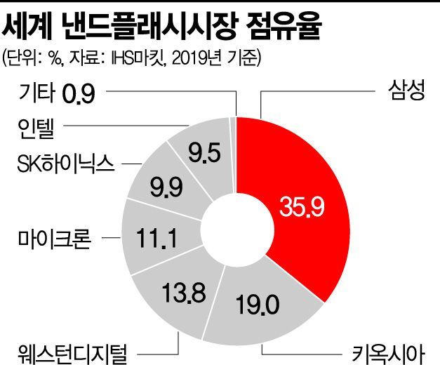
According to IHS Markit, as of last year, Samsung Electronics holds a dominant 35.9% share of the global NAND flash market, ranking first. It is followed by Kioxia (19%), Western Digital (13.8%), Micron (11.1%), SK Hynix (9.9%), and Intel (9.5%). An Gi-hyun, executive director of the Korea Semiconductor Industry Association, said, "Demand for NAND flash is expected to increase exponentially in the untact (contactless) society," adding, "NAND is a market with fiercer competition led by the top six companies compared to DRAM, and Samsung Electronics' preemptive establishment of domestic production facilities is an aggressive investment to maintain its global super-gap."
© The Asia Business Daily(www.asiae.co.kr). All rights reserved.


