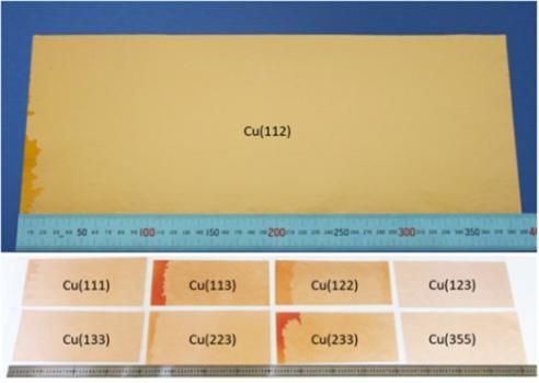
 The joint research team synthesized large-area single-crystal thin films with high Miller indices, which were previously difficult to synthesize. In this study, a high Miller index means that the value of each index exceeds 1. The Miller index is an index that represents the pattern of a metal substrate.
[Asia Economy Reporter Junho Hwang] Domestic researchers have succeeded in diversifying the surface patterns of metal substrates used for synthesizing two-dimensional materials in flexible and rollable electronic devices. They have secured technology to synthesize single-crystal metal thin films with over 30 different surface patterns on a large scale, which is expected to enable the development of two-dimensional materials with various patterns. On the 28th, the Ministry of Science and ICT announced that the research results of the Funding Group Leader's team from the Multidimensional Carbon Materials Research Group at the Institute for Basic Science (IBS) were published in the international academic journal Nature.
This study is an advancement of last year's research, which revealed that metal substrates used in manufacturing two-dimensional single-crystal materials such as graphene hold the key to large-area single-crystal materials. The research team identified that the orientation of the synthesized material varies depending on the substrate's pattern and previously proposed a method to synthesize metal substrates with various patterns. Two-dimensional single-crystal materials have a regular atomic arrangement and orientation. They exhibit excellent thermal and electrical conductivity, making them materials for high-performance electronic devices.
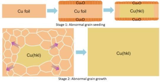
The research team cut copper single crystals to obtain fragments (seeds) with desired patterns. These were then attached to polycrystalline copper and annealed at a high temperature close to the melting point (1020℃). Annealing is a process of heating to a certain temperature and then slowly cooling to homogenize the internal structure and change physical properties. As a result, the crystals around the fragments rearranged into the same pattern as the fragments and gradually expanded over a wider area. They confirmed that the entire thin film eventually transformed into a single crystal with the same pattern.
The research team stated that by utilizing this technology, it has become possible to synthesize metal thin films with various surface patterns on a large scale. With a wider selection of substrates, it is now possible to control the orientation of the material to be synthesized, enabling high-performance two-dimensional materials with desired properties.
Funding, group leader at the Institute for Basic Science (IBS), said, "The production of large-area single-crystal metal thin films with various crystal planes has been a long-standing challenge in the field of materials science." He added, "The large-area single-crystal metal thin films synthesized through this research can be used in various ways, such as molds for synthesizing various single-crystal two-dimensional materials and catalysts that selectively trigger specific chemical reactions."
 It is the formation mechanism of large-area single-crystal copper thin films with a high Miller index.
© The Asia Business Daily(www.asiae.co.kr). All rights reserved.


