Large-scale Investment in System Semiconductors
TSMC, the World's Top Foundry, Closely Chased
Construction Starts This Month, Operation Begins in Second Half of Next Year
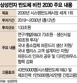
[Asia Economy Reporter Kim Hyewon] Samsung Electronics is building a foundry (semiconductor contract manufacturing) facility in Pyeongtaek following Giheung and Hwaseong in Gyeonggi Province to respond to the increasing demand for cutting-edge products based on extreme ultraviolet (EUV) technology. This is part of the 'Semiconductor Vision 2030' strategy, which aims to become the world’s number one in the system semiconductor sector by 2030. Samsung Electronics plans to accelerate its pursuit of the world’s top company, Taiwan’s TSMC, based on its foundry lines in Pyeongtaek, Giheung, and Hwaseong.
On the 21st, Samsung Electronics announced that it has decided to build an EUV foundry line in Pyeongtaek, focusing mainly on products below 5 nanometers, and began construction this month. The scheduled operation date is the second half of 2021. Although Samsung Electronics did not disclose the exact investment scale, the industry expects that around 10 trillion won will be invested in the EUV foundry production facilities to be established in the P2 line of the Pyeongtaek plant.
Regarding this new domestic investment in the system semiconductor sector, Samsung Electronics Vice Chairman Lee Jae-yong reportedly reiterated to the management team, "We must not stop investing in the future, especially in difficult times."
With this, Samsung Electronics aims to expand its foundry footprint to Pyeongtaek following the start of operations at the EUV-exclusive Hwaseong V1 line in February, increasing the application range of ultra-fine process technology across various fields such as mobile, high-performance computing (HPC), and artificial intelligence (AI). Since announcing Semiconductor Vision 2030 last April, Samsung Electronics has been executing detailed step-by-step strategies to achieve global number one status in the system semiconductor sector.
Since beginning mass production of 7-nanometer products using the industry’s first EUV process at the Hwaseong S3 line last April, Samsung Electronics has continuously expanded ultra-fine process production capacity through the V1 line earlier this year. With mass production starting at the Pyeongtaek line in 2021, the production volume of products based on ultra-fine processes below 7 nanometers is expected to increase sharply. Samsung Electronics also plans to begin mass production of 5-nanometer products first at Hwaseong in the second half of this year, followed by making them the main production focus at the Pyeongtaek foundry line in the future.
Jung Eun-seung, President of Samsung Electronics’ DS Division Foundry Business, emphasized, "We will actively respond to the increasing demand in the ultra-fine market based on EUV by expanding the production scale of products below 5 nanometers. Through strategic investment and continuous recruitment, we will maintain solid growth in the foundry business."
© The Asia Business Daily(www.asiae.co.kr). All rights reserved.


