A new fabrication technology has been developed that enables the high-density placement of nano lasers on semiconductor chips. Nano lasers make it possible to process information with light in spaces thinner than a strand of hair. In advanced industries such as ultra-fast optical computing for large-scale artificial intelligence (AI) operations and quantum cryptography communications, nano lasers are gaining attention as a next-generation core component for semiconductors.

KAIST announced on January 6 that the research team led by Professor Kim Ji-Tae from the Department of Mechanical Engineering, in collaboration with the research team of Professor Noh Junseok at POSTECH, has developed an ultra-fine three-dimensional printing technology capable of producing "vertical nano lasers," a key component for ultra-high-density photonic integrated circuits.
The conventional semiconductor manufacturing method, known as the lithography process, is effective for mass-producing identical structures. However, due to its complexity and high cost, it is difficult to freely change the shape or position of components.
Additionally, traditional lasers are fabricated in a horizontal structure laid flat on a substrate, which takes up a lot of space and suffers from reduced efficiency as light leaks downward.
To address these issues, the joint research team developed a new 3D printing method that vertically stacks "perovskite," a next-generation semiconductor material capable of efficiently generating light. This is an "ultra-fine electrohydrodynamic 3D printing" technology that precisely controls minuscule ink droplets (attoliters) using voltage.
Using this technology, the joint research team succeeded in directly printing hair-thin, pillar-shaped nano structures vertically at desired locations, without the need for complex material removal processes. Most notably, the surface of the printed perovskite nano structures is extremely smooth, significantly enhancing laser efficiency.
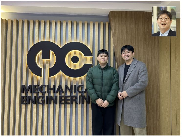 (From left) Professor Ji-Tae Kim of KAIST, Dr. Shuichi (first author, AI-Based Intelligent Design-Manufacturing Integration Research Group, KAIST-POSTECH), Professor Jun-Seok Noh of POSTECH. Provided by KAIST
The joint research team also combined a vapor-phase crystallization control technique during the printing process to achieve a high-quality structure with crystals aligned in a single direction. As a result, they emphasized that they were able to realize a "high-efficiency vertical nano laser" that operates stably while minimizing light loss.
They further demonstrated that by adjusting the height of the nano structures, the color of the laser light can be precisely tuned. According to the joint research team, this could enable the production of laser security patterns that are invisible to the naked eye and can only be detected with special equipment, making the technology highly promising for commercialization as an anti-counterfeiting solution.
Professor Kim stated, "This technology is significant in that it enables the direct, high-density implementation of light-based computing semiconductors on chips without complex processes," adding, "It is also expected to contribute to accelerating the commercialization of ultra-fast optical computing and next-generation security technologies."
© The Asia Business Daily(www.asiae.co.kr). All rights reserved.


