UNIST and Ajou University Develop Low-Power Terahertz Quantum Tunneling Device with Solved Heat Issues
Stable Operation for 1,000 Cycles... Paving the Way for Next-Generation 6G and Quantum Device Commercialization, Published in ACS Nano
A new quantum device with ultra-high-speed operation capabilities, essential for 6G communications and other applications, has been developed.
The research team led by Professor Hyungryul Park from the Department of Physics at UNIST, in collaboration with Professor Sangwoon Lee's team from the Department of Physics at Ajou University, announced on December 30 that they have developed a new terahertz quantum device that overcomes the issue of conventional quantum devices melting under strong electric fields.
 Research team: Professor Hyungryul Park of UNIST, Professor Sangwoon Lee of Ajou University, Researcher Gangseon Ji of UNIST (first author). Provided by UNIST
The terahertz quantum device is considered a next-generation component that enables ultra-high-speed signal processing, such as 6G communications, which is difficult to achieve with the slow operating speed of conventional semiconductors.
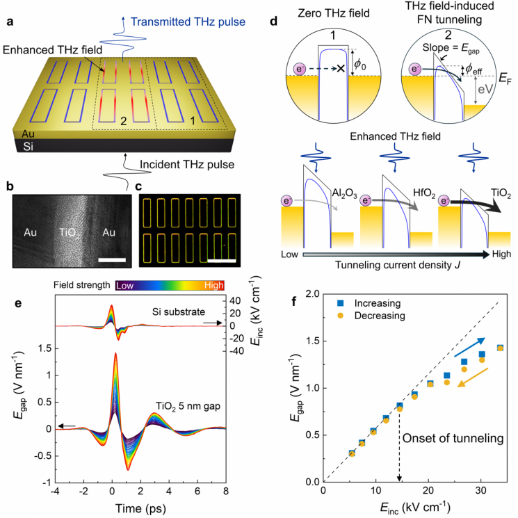
This is made possible by utilizing electron tunneling induced by terahertz waves, which oscillate trillions (10¹²) of times per second. Tunneling is a quantum phenomenon in which electrons pass through an energy barrier.
The challenge has been that to induce tunneling, an extremely strong terahertz electric field of 3 V/nm (volts per nanometer) must be applied. Such a strong electric field causes heat generation, which leads to the melting of the device's metal electrodes or damage to its structure.
The research team developed a terahertz quantum device in which tunneling occurs efficiently even under an electric field about one-fourth as strong as before. The terahertz quantum device consists of an insulator sandwiched between metal electrodes, and the team replaced the conventional aluminum oxide (Al₂O₃) insulator with titanium dioxide (TiO₂). This technology leverages the principle that using titanium dioxide lowers the height of the energy barrier.
First author Gangseon Ji explained, "Rather than pushing electrons with a strong electric field, we adopted an approach that opens a pathway for electrons to move more easily. Since tunneling is a probabilistic phenomenon, lowering the energy barrier height causes the probability to increase rapidly."
The research team fabricated high-quality devices with this structure using an optimized atomic layer deposition process. Normally, when depositing a titanium dioxide thin film on metal electrodes, defects such as tiny atomic-scale holes (oxygen vacancies) are prone to occur.
Professor Sangwoon Lee of Ajou University stated, "By applying the latest atomic layer deposition technology used in mass production processes for semiconductor logic and memory devices, we were able to eliminate oxygen vacancy defects in next-generation quantum devices." Atomic layer deposition is a technique in which precursor gases are alternately injected to deposit thin films one atomic layer at a time on a substrate.
The developed device demonstrated stable tunneling operation even at an electric field of about 0.75 V/nm. In addition, thanks to the excellent heat dissipation properties of titanium dioxide, the device operated stably without any performance degradation for over 1,000 cycles, even under conditions where the terahertz wave transmittance was adjusted up to 60%.
Professor Hyungryul Park of UNIST emphasized, "We have fundamentally solved the biggest obstacles to the commercialization of terahertz quantum devices-high-voltage operation and thermal destruction. This will become a core technology not only for future optical communication devices beyond the 6G era, but also for highly sensitive quantum sensing applications."
This research was published online on December 20 (local time) in ACS Nano, a world-renowned journal in the field of nanoscience. The study was supported by the National Research Foundation of Korea (NRF) and the Institute for Information & Communications Technology Planning & Evaluation (IITP) under the Ministry of Science and ICT.
© The Asia Business Daily(www.asiae.co.kr). All rights reserved.
![Clutching a Stolen Dior Bag, Saying "I Hate Being Poor but Real"... The Grotesque Con of a "Human Knockoff" [Slate]](https://cwcontent.asiae.co.kr/asiaresize/183/2026021902243444107_1771435474.jpg)


