Chairman Jay Y. Lee Visits Giheung and Hwaseong Sites
Positive Signal for HBM4 Supply, Employee Morale Boost
Emphasizing 'Leadership' Amid Semiconductor Industry's Shift to AI
Samsung Electronics Chairman Jay Y. Lee has been visiting key domestic semiconductor sites in succession, emphasizing the need to restore technological competitiveness. As the global semiconductor industry is shifting toward artificial intelligence (AI), his actions are interpreted as a signal of Samsung's intention to continue investing and innovating across all sectors, from memory to foundry and system semiconductors.
According to the industry on December 23, Chairman Lee visited 'NRD-K,' a next-generation semiconductor research and development (R&D) complex within the Samsung Electronics Giheung Campus the previous day to inspect the status of its R&D facilities. NRD-K is a state-of-the-art integrated research complex established by Samsung Electronics to secure leadership in future semiconductor technologies, serving as a hub to strengthen technological competitiveness across all business areas, including memory, foundry, and system semiconductors. During his visit, Chairman Lee reviewed the progress of major products and technology development. Later in the afternoon, he visited the Hwaseong Campus to check on the implementation of manufacturing automation systems such as digital twins and robots, as well as the current use of AI technologies.
At the site, Chairman Lee met with key executives including Jeon Younghyun, Head of the Device Solutions (DS) Division, and Song Jaehyuk, Chief Technology Officer (CTO) of the DS Division, to discuss semiconductor business trends and future strategies. He also listened to feedback from employees who contributed to the commercialization of cutting-edge semiconductor products such as high bandwidth memory (HBM), D1c, and V10.
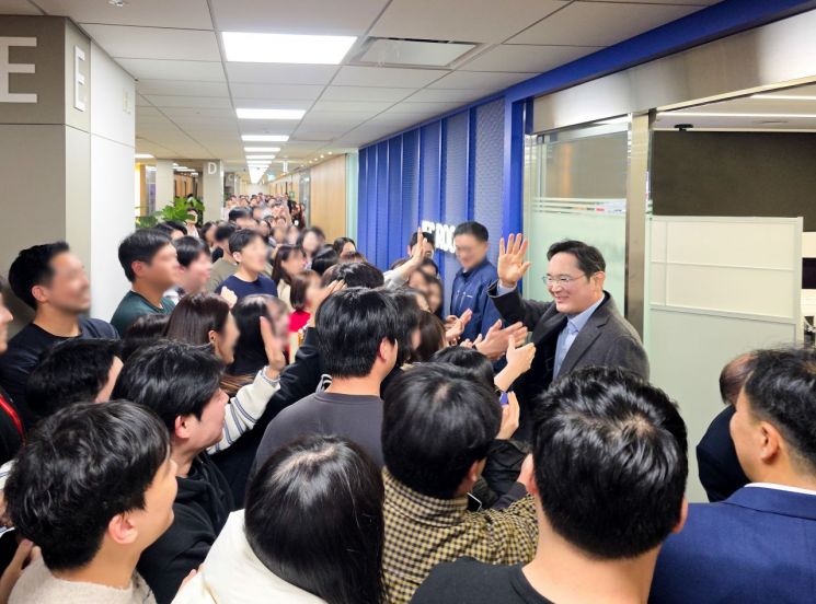 Samsung Electronics Chairman Jay Y. Lee is greeting employees during his visit to the Samsung Electronics Hwaseong Campus on the 22nd. Samsung Electronics.
Chairman Lee's decision to visit a semiconductor site following his visit to the Samsung Biologics Songdo Campus in Incheon this June is seen as an effort to boost the morale of employees at semiconductor sites, whose performance has significantly improved in the second half of the year. Samsung Biologics recorded strong results last year, with consolidated sales exceeding 4 trillion won.
Similarly, from the third quarter of this year, Samsung Electronics began to show signs of recovery in its semiconductor business by increasing shipments of HBM. In addition, the global expansion of AI infrastructure investments led to a rise in general DRAM prices, resulting in high operating profits. The securities industry forecasts that the operating profit of Samsung Electronics' memory business division will surge to over 23 trillion won in the second half of the year.
Furthermore, Samsung Electronics has recently received high marks from Nvidia for its sixth-generation high bandwidth memory, HBM4, raising expectations for supplying HBM4 to Nvidia next year.
At the site, Chairman Lee reportedly urged, "Let us restore our fundamental technological competitiveness through bold innovation and investment." This visit is being interpreted as more than just an on-site encouragement, but as an effort to share a sense of crisis within the company regarding the current state of Samsung's semiconductor business. Recently, as the profitability of general-purpose memory and legacy processes has weakened, the center of gravity in the semiconductor industry has been shifting rapidly to AI-critical areas such as HBM and advanced ultra-fine processes.
Industry experts are also focusing on Samsung Electronics' foundry competitiveness as a key factor behind the positive evaluation of HBM4. In the high bandwidth memory race, not only the performance of memory chips but also their compatibility with logic semiconductor processes has emerged as a critical variable. Samsung Electronics' next-generation HBM4 is said to have received high marks for power efficiency and signal stability, thanks to an internal collaborative structure that simultaneously optimizes both logic and memory processes.
Another strength is that the company can adjust memory interfaces and packaging structures from the design stage by incorporating foundry process requirements. Based on its vertically integrated structure, which encompasses both memory and foundry, Samsung can quickly implement process changes and technical enhancements.
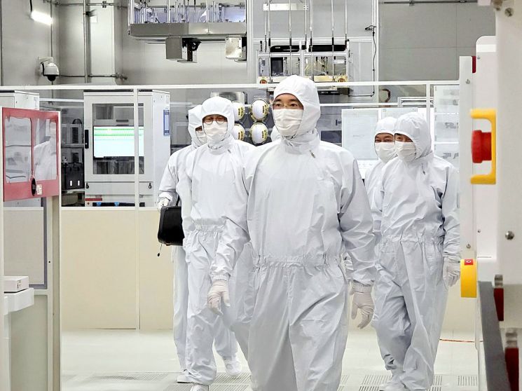 Samsung Electronics Chairman Lee Jae-yong is inspecting the NRD-K cleanroom facility, an advanced integrated semiconductor research and development (R&D) center, located within the Samsung Electronics Giheung Campus on the 22nd. Samsung Electronics.
This aligns with Samsung Electronics' strategy to directly manage and enhance competitiveness across the entire process, from design to manufacturing, not only for memory but also for foundry and system semiconductors. In fact, when asked by foreign media last year about the possibility of spinning off the foundry or system semiconductor business, Chairman Lee drew a clear line, stating, "There is a strong desire to scale up the business." The industry now expects that the foundry business, which had been operating at a loss, could see improved profitability as demand for high-value-added products grows in tandem with the semiconductor supercycle.
An industry official commented, "Base die technology based on the 4-nanometer process (foundry) is also playing an important role in restoring HBM4 competitiveness," adding, "It appears that Samsung is continuing to invest in foundry and nurturing it as a future growth engine." Especially as competition with global semiconductor companies intensifies, it is necessary to enhance overall competitiveness not only in memory but also in system semiconductors and foundry.
Kim Yongseok, Distinguished Professor at Gachon University’s College of Semiconductor, explained, "This can be interpreted as a directive to reestablish clear technological leadership in the AI memory sector, with HBM as the starting point." He added, "As competition continues in next-generation HBM and CXL for AI semiconductor memory, the directive calls for comprehensive system capability enhancements, including improving foundry yield, automating manufacturing through AI factories, and boosting productivity-not just in memory, but across the board."
© The Asia Business Daily(www.asiae.co.kr). All rights reserved.


