Professor Suhyun Kim's Team Develops Ruthenium Precursor Stable Even at 400°C
High-Temperature ALD Process Achieves Both Wiring Quality and Speed, Published in Adv. Sci.
Semiconductor wiring is now thinner than a human hair. The problem lies with the electric current. As the wiring becomes thinner, resistance increases dramatically.
A new material has been developed to address the so-called "electrical arteriosclerosis" phenomenon that occurs as the width of semiconductor circuit lines decreases.
On December 18, the research team led by Professor Suhyun Kim at the Graduate School of Semiconductor Materials and Components at UNIST announced the development of a new precursor material for ruthenium, a next-generation semiconductor wiring material, as well as an atomic layer deposition (ALD) process applying this precursor.
 Research team, (from left) Professor Suhyun Kim, Researcher Hideaki Nakatsubo (first author), Professor Debananda Mohapatra, Researcher Jeongha Kim. Provided by UNIST
Metal wiring is a core structure that supplies power and transmits signals to the hundreds of millions of transistors inside a semiconductor chip.
As manufacturing processes become more refined, wiring widths are shrinking. For conventional copper wiring, as the line width decreases, the electrical resistance of the thin film increases sharply, impeding current flow and leading to reduced chip performance. In contrast, ruthenium exhibits a much milder increase in resistance as the line width narrows, making it a promising next-generation wiring material. Additionally, unlike copper, ruthenium does not require a separate diffusion barrier layer, allowing for a simpler structure.
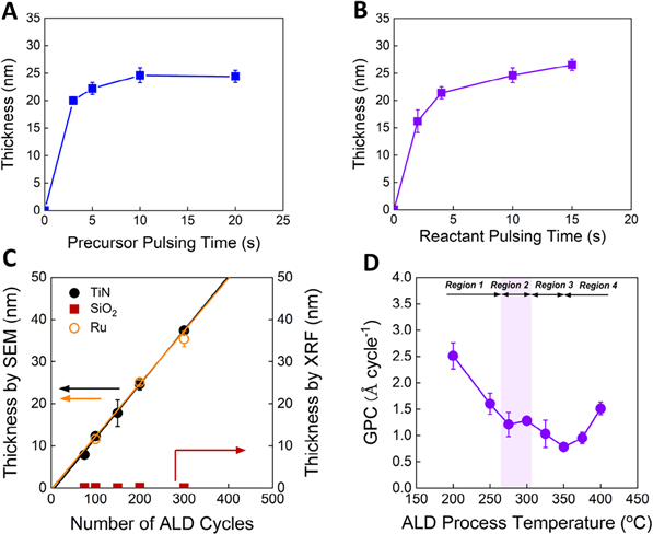
The precursor material developed by the research team does not decompose even at 400°C, enabling the formation of high-quality ruthenium wiring. The ruthenium wiring is formed by first adsorbing the precursor onto the substrate, then injecting a reactive gas to remove all parts except the ruthenium metal portion of the precursor, using the ALD method. While higher process temperatures improve wiring quality, existing ruthenium precursors could not withstand such temperatures and would decompose. The new precursor overcomes this limitation.
The ruthenium thin film deposited with this precursor achieved a low resistivity of 10.6 micro-ohm-centimeters (μΩ·cm), which is very close to the ideal bulk value of 7.4 μΩ·cm, even without heat treatment. It also recorded over 95% step coverage, meaning that thin films can be uniformly coated even on narrow and deep semiconductor structures such as 3D NAND.
 Experimental results of ALD thin film deposition process using developed ruthenium precursor (raw material).
The precursor material used in this research can also reduce semiconductor processing costs and time. This is because ruthenium is selectively deposited only where wiring is needed and does not adhere to insulators where conductivity is not required. In the past, wiring that adhered to insulators had to be removed through a separate etching process. Additionally, the process produced a ruthenium thin film with a thickness of 0.13 nanometers (nm, 1.28 angstroms) per cycle, which is about twice as fast as previous methods.
Professor Suhyun Kim stated, "As the integration density of semiconductor devices increases, the difficulty of wiring processes is rising exponentially. It is significant that we have simultaneously achieved reduced resistance for fine line widths, uniform deposition on 3D structures, and faster deposition speeds. This will contribute to improving the yield and performance competitiveness of next-generation logic and memory semiconductor mass production processes."
This research was conducted as an international collaboration between UNIST and TANAKA PRECIOUS METAL TECHNOLOGIES Co., Ltd., a Japanese precious metal materials company. The results were published online in the renowned international journal Advanced Science on November 23.
The research was supported by the Technology Innovation Program of the Ministry of Trade, Industry and Energy (MOTIE).
© The Asia Business Daily(www.asiae.co.kr). All rights reserved.


