 (From left) Professor Hong Sungmin of the Department of Electrical Engineering and Computer Science at GIST, researchers Lee Kwangun, Kim Inki, Jung Seungwoo, and Jang Minseo.
Gwangju Institute of Science and Technology (GIST) announced on October 16 that a research team led by Professor Hong Sungmin from the Department of Electrical, Electronics and Computer Engineering has developed a new algorithm that can predict the performance of next-generation semiconductor devices at speeds up to 100 times faster than conventional methods, dramatically improving the computational efficiency of semiconductor device simulations.
This achievement is significant because it fundamentally solves the problem of "lengthy simulations," which has long been considered the biggest obstacle in semiconductor device research and development (R&D) processes.
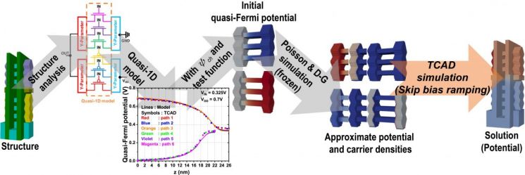
In order to predict and optimize the performance of semiconductor devices in advance, "TCAD simulation" is essential. TCAD is a technology that numerically calculates the movement of electrons and holes inside semiconductors and the distribution of electric fields according to physical laws, enabling precise prediction of the electrical characteristics of devices. However, complex next-generation devices such as the latest gate-all-around (GAA) structures or complementary field-effect transistors (CFETs) require three-dimensional calculations, resulting in simulations that can take hours or even days. This has significantly slowed down the pace of research and development.
In particular, to ensure stable calculations at the desired voltage conditions, a "bias-ramping" process-which gradually increases the voltage to induce convergence-was essential. This process accounted for most of the total computation time and acted as a bottleneck.
Recently, there have been attempts to use trained artificial neural network (ANN)-based artificial intelligence (AI) models to generate excellent initial estimates and reduce unnecessary intermediate steps. However, when applying these approaches to new structures, additional data and training processes are required, making immediate industrial application difficult.
To address these challenges, the research team proposed a new approach that combines "quasi-one-dimensional (Quasi-1D) modeling" with "region-wise structure analysis." This method can significantly reduce the time required for semiconductor device simulations without any pre-training process. The core idea is to simplify complex semiconductor devices into a one-dimensional model along the channel direction where current flows, enabling rapid estimation of initial solutions. The device is divided into multiple regions, and the optimal physical model is applied to each region. Through this, the previously essential bias-ramping process can be omitted, while achieving calculation speeds 10 to 100 times faster than before.
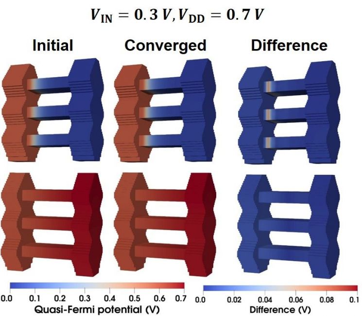 Comparison of the initial quasi-Fermi potential of the quasi one-dimensional model (left) and the converged quasi-Fermi potential from the semiconductor device simulation (center).
The research team validated the new algorithm on various next-generation devices, including gate-all-around (GAA) devices and complementary field-effect transistor (CFET) inverters. As a result, simulation speeds improved by more than 10 to 100 times compared to conventional methods, and the error in key electrical characteristics such as voltage transfer characteristics (VTC) was suppressed to less than 0.1 volts (V) compared to previous TCAD results, demonstrating high accuracy. In addition, the algorithm consistently produced stable results even when the device geometry or mesh conditions-referring to the small regions divided during the computation process-were changed, showing no performance degradation. This confirms that the method can be reliably applied in various environments and structures.
Professor Hong Sungmin stated, "This research demonstrates that even without pre-trained ANN-based AI models, it is possible to drastically shorten semiconductor device simulation times across a variety of structures. Based on the efficiency, accuracy, and stability of the proposed technique, we expect it will accelerate the development of next-generation semiconductor devices and enhance research efficiency moving forward."
This study, supervised by Professor Hong Sungmin and conducted by researchers Lee Kwangun, Kim Inki, Jung Seungwoo, and Jang Minseo from the Department of Electrical, Electronics and Computer Engineering at GIST, was supported by the Individual Basic Research Program (Mid-Career) of the Ministry of Science and ICT and the National Research Foundation of Korea. The research results were published online in the international journal "Communications Engineering" on September 25.
© The Asia Business Daily(www.asiae.co.kr). All rights reserved.
![Clutching a Stolen Dior Bag, Saying "I Hate Being Poor but Real"... The Grotesque Con of a "Human Knockoff" [Slate]](https://cwcontent.asiae.co.kr/asiaresize/183/2026021902243444107_1771435474.jpg)


