SK Hynix Secures Leadership in the AI Memory Market
Completes Mass Production Readiness Just Six Months After Sample Supply
Samsung Electronics Bets on Advanced Process Technology for Performance Advantage
SK Hynix has become the world's first company to begin mass production of the 6th generation High Bandwidth Memory (HBM4). By moving ahead of Samsung Electronics and Micron, who are still in the sample supply stage, SK Hynix is further strengthening its leadership position in the next-generation artificial intelligence (AI) memory market. However, some predict that the landscape could shift depending on Samsung Electronics' yield stabilization, mass production timing, and the results of Nvidia's qualification tests, as Samsung is applying more advanced processes to its logic and core dies.
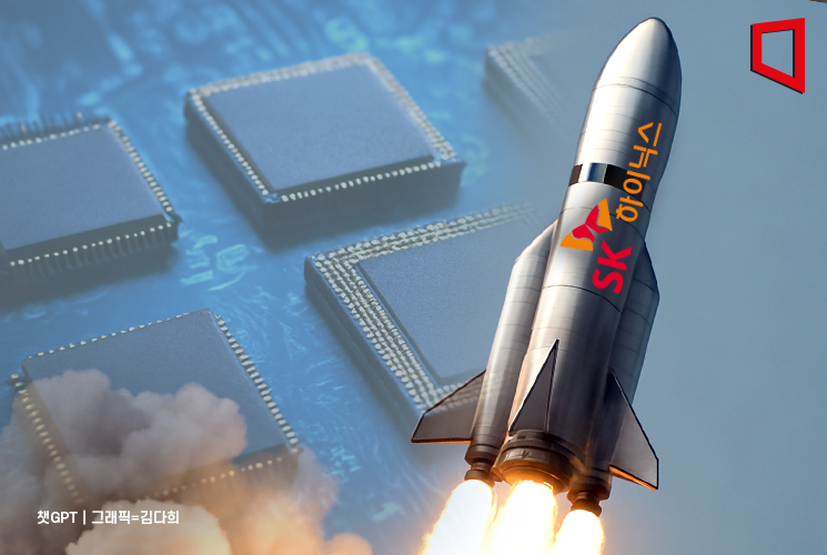
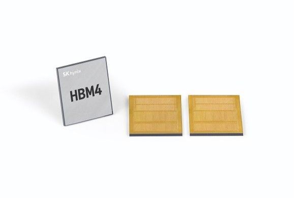
On the 12th, SK Hynix announced that it has completed the development of HBM4 and established the world's first mass production system. HBM is a high-performance, high-value product that stacks multiple DRAM chips vertically to dramatically increase data processing speeds. In March of this year, SK Hynix supplied HBM4 12-layer samples to customers, and within six months, completed preparations for mass production. By being the first to commercialize this technology ahead of its competitors, SK Hynix is being recognized for securing the initiative in the next-generation memory market.
With the rapid advancement of the AI industry and infrastructure, demand for data computation and processing is surging. This is why demand for HBM continues to grow steadily, as it enables faster system speeds. The heavy power consumption required to operate data centers has also made securing memory power efficiency a core priority for companies.
The HBM4 that SK Hynix is set to mass-produce features 2,048 data transmission channels (I/O), which is double that of the previous generation. This has doubled the bandwidth and improved power efficiency by more than 40%. SK Hynix forecasts that introducing this product into customer systems can enhance AI service performance by up to 69%, fundamentally resolving data bottlenecks while also significantly reducing data center power costs.
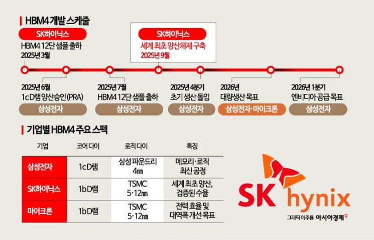
Furthermore, the new HBM4 achieves operating speeds exceeding 10Gbps (10 gigabits per second), far surpassing the JEDEC (Joint Electron Device Engineering Council) standard operating speed of 8Gbps. During development, SK Hynix applied its proprietary bonding and molding process (MR-MUF) and incorporated 5th generation 1b DRAM at the 10nm (1nm = one-billionth of a meter) class, ensuring high reliability.
By being the first to enter mass production, SK Hynix is expected to secure a competitive advantage in supplying major customers such as Nvidia, in line with its long-standing "Time to Market" principle. Rival Samsung Electronics is targeting mass production as early as the fourth quarter of this year, while US-based Micron is aiming for large-scale production next year, highlighting a significant gap.
Kim Joosun, President of AI Infrastructure and Chief Marketing Officer (CMO) at SK Hynix, stated, "HBM4, for which we have announced the world's first mass production system, marks a symbolic turning point that surpasses the limits of AI infrastructure. We will continue to supply the highest quality memory required in the AI era in a timely manner and grow into a 'full-stack AI memory provider.'"
 SK Hynix has become the world's first to begin mass production of the 6th generation High Bandwidth Memory (HBM4). SK Hynix
With SK Hynix quickly establishing a mass production system, competition is expected to intensify further.
Samsung Electronics is aiming for a turnaround in the HBM4 market, which is set to take off in earnest next year. To this end, the company has taken a bold step by applying even more advanced processes. For the "logic die," which serves as the brain of HBM, Samsung is using its foundry's 4nm process, and for the core die (DRAM), it plans to use a next-generation 1c DRAM. In contrast, SK Hynix and Micron are producing logic dies using Taiwan's TSMC 5nm or 12nm processes and are utilizing 1b DRAM as the core die.
The semiconductor industry is closely watching how Samsung Electronics' strategy will play out. Nvidia, its largest customer, is preparing to launch "Rubin," the successor to next year's AI accelerator Blackwell series. In this context, it has recently been reported that Nvidia has requested memory manufacturers to "increase HBM4 data processing speeds."
The key for Samsung Electronics lies in quickly securing the performance and yield of the 1c DRAM to be used as the HBM4 core die. At the end of June, Samsung Electronics succeeded in developing the 1c DRAM and completed mass production approval (PRA).
© The Asia Business Daily(www.asiae.co.kr). All rights reserved.
![Clutching a Stolen Dior Bag, Saying "I Hate Being Poor but Real"... The Grotesque Con of a "Human Knockoff" [Slate]](https://cwcontent.asiae.co.kr/asiaresize/183/2026021902243444107_1771435474.jpg)


