Participation in IEEE VLSI Symposium 2025
Miniaturization with Existing DRAM Technology Reaches Its Limits
Transition to 4F² VG Platform at Sub-10-Nanometer Scale
"Working with the Industry to Make the Future a Reality"
SK Hynix announced on June 10 that it officially unveiled its next-generation DRAM technology roadmap, which will guide the company for the next 30 years, at the 'IEEE VLSI Symposium 2025' held in Kyoto, Japan from June 8 to 12. This roadmap presents a blueprint for advancing the company's DRAM technology. It also signals SK Hynix's determination to maintain its momentum after achieving the top position in the DRAM market share for the first time in the first quarter of this year.
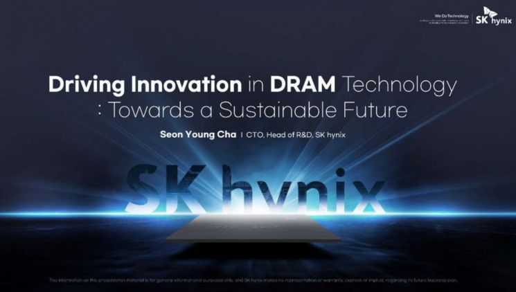
The roadmap was presented by Chae Sun Yong, Head of Future Technology Research Institute (Chief Technology Officer, CTO) at SK Hynix, who delivered the keynote speech at the event. The theme was 'Leading DRAM Technology Innovation for a Sustainable Future.' Chae pointed out, "The current microfabrication processes based on today's tech platforms are reaching a stage where it is becoming increasingly difficult to improve performance and capacity." He added, "To overcome these challenges, we will break through technological limitations by preparing '4F² VG Platform' and '3D DRAM' technologies, which are based on innovations in structure, materials, and components at the sub-10-nanometer (nm; 1 nm is one-billionth of a meter) scale."
A tech platform refers to a technological framework that can be applied across multiple generations. The '4F² VG Platform' is a next-generation memory technology that minimizes the cell area of DRAM and enables high density, high speed, and low power DRAM through a vertical gate structure. F² represents the area occupied by a single DRAM cell that stores data, and F refers to the minimum line width of a semiconductor. Thus, 4F² means that one cell occupies an area of 2F x 2F, which is a high-density technology to fit more cells onto a single chip. VG (Vertical Gate) is a structure where the gate, which acts as a transistor switch in DRAM, stands vertically and is surrounded by the channel. Traditionally, the gate was laid horizontally on top of the channel in a planar structure. While 6F² cells are currently common, applying wafer bonding technology?placing the circuitry below the cell area along with 4F² cells?can be expected to improve not only cell efficiency but also electrical characteristics.
Alongside 4F² VG, Chae also presented 3D DRAM as a core pillar of next-generation DRAM technology. While the industry is concerned that manufacturing costs for this technology could increase in proportion to the number of stacked layers, SK Hynix has set a strategy to overcome this through technological innovation and secure competitiveness. The company also announced plans to advance key materials and all DRAM components, thereby securing new growth engines and establishing a foundation for the continued evolution of DRAM technology over the next 30 years.
 Image material from the keynote speech by Chason Yong, Head of Future Technology Research Institute at SK Hynix, at IEEE VLSI 2025. Photo by SK Hynix
Chae stated, "Around 2010, there were many predictions that 20-nanometer DRAM technology would be the limit, but we have reached where we are today through continuous technological innovation." He added, "We will present a mid- to long-term vision for technological innovation that will serve as a milestone for young engineers who will participate in DRAM technology development in the future, and we will work together with the industry to make the future of DRAM a reality."
The industry is paying close attention to whether SK Hynix can realize these roadmaps as planned and further solidify its position as the number one DRAM manufacturer. According to market research firm TrendForce, SK Hynix ranked first in global DRAM market share (by revenue) in the first quarter of this year with 36.0%. Its revenue reached $9.7 billion.
Meanwhile, the IEEE VLSI Symposium, which SK Hynix chose as the stage to announce its next-generation DRAM technology, is recognized as the world's most prestigious academic conference in the field of semiconductor circuit and process technology. It is held alternately in the United States and Japan every year. The latest research achievements in next-generation semiconductors, AI chips, memory, and packaging are presented at the event. On the final day of the event, June 12, Park Judong, Executive Vice President of SK Hynix (Head of Next-Generation DRAM Task Force), is scheduled to present the latest research results on the electrical characteristics of DRAM achieved by applying VG and wafer bonding technologies.
© The Asia Business Daily(www.asiae.co.kr). All rights reserved.

![User Who Sold Erroneously Deposited Bitcoins to Repay Debt and Fund Entertainment... What Did the Supreme Court Decide in 2021? [Legal Issue Check]](https://cwcontent.asiae.co.kr/asiaresize/183/2026020910431234020_1770601391.png)


