 Yongin Semiconductor Industrial Complex Integrated Water Supply Project Plan Layout. Photo by Ministry of Environment
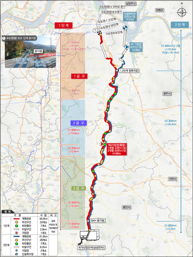
The Ministry of Environment announced on May 16 that it will begin the basic and detailed design phase for the first stage of the 'Yongin Semiconductor Industrial Complex Integrated Water Supply Project.'
The Yongin Semiconductor Industrial Complex is the world's largest semiconductor cluster, housing companies such as Samsung Electronics (National Industrial Complex) and SK Hynix (General Industrial Complex). The Ministry of Environment is building infrastructure to supply 1,072,000 tons (㎥) of water, investing a total project cost of 2.2 trillion won by 2034. The project will be carried out in two phases according to water demand: Phase 1 (310,000 ㎥/day by 2031) and Phase 2 (762,000 ㎥/day by 2035).
This basic and detailed design phase covers the first stage of the project, which includes constructing a dedicated pipeline of 46.9 km from Paldang Dam to Yongin and building one booster station. The Ministry of Environment completed the basic plan in June last year and the feasibility study from July last year to February this year. The design phase, starting today, is expected to take about one year and six months, until November next year. Construction will then proceed until 2030, with actual water supply beginning in January 2031.
Kim Hyojung, Director of Water Use Policy at the Ministry of Environment, stated, "Supplying industrial water sufficiently and in a timely manner is a core responsibility of the nation," adding, "We will closely coordinate with relevant agencies and provide maximum support to ensure the project progresses rapidly."
© The Asia Business Daily(www.asiae.co.kr). All rights reserved.

![Clutching a Stolen Dior Bag, Saying "I Hate Being Poor but Real"... The Grotesque Con of a "Human Knockoff" [Slate]](https://cwcontent.asiae.co.kr/asiaresize/183/2026021902243444107_1771435474.jpg)


