Established 'Advanced Packaging Equipment Development Center'
Focusing on the development of new technologies such as hybrid bonding
Hanwha Semitek announced on May 1 that it has carried out an organizational restructuring to strengthen its capabilities, including establishing a dedicated unit for the development of next-generation semiconductor equipment and significantly increasing its technical workforce.
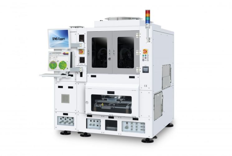
As part of this restructuring, the company created the 'Advanced Packaging Equipment Development Center.' The center plans to focus on developing new technologies such as hybrid bonding.
Previously, in March, Hanwha Semitek succeeded in mass-producing TC bonders worth 42 billion KRW, joining the 'Nvidia supply chain.' The company explained that this organizational restructuring reflects its intention to respond to the surging demand for TC bonders and to develop next-generation technologies that could lead the global market in the future. There is also attention on whether Hanwha Semitek will achieve tangible results in the 'fluxless' and hybrid bonding sectors, which are considered post-TC bonding technologies.
A Hanwha Semitek representative stated, "With this organizational restructuring, we have secured new momentum to lead the next-generation HBM semiconductor equipment market," adding, "We will continue to expand our investment in research and development (R&D) to drive technological innovation."
© The Asia Business Daily(www.asiae.co.kr). All rights reserved.

![Clutching a Stolen Dior Bag, Saying "I Hate Being Poor but Real"... The Grotesque Con of a "Human Knockoff" [Slate]](https://cwcontent.asiae.co.kr/asiaresize/183/2026021902243444107_1771435474.jpg)


