2nm Process Pilot Production in Taiwan
Showcasing Technology to Pressure Competitors
Japan's No.1 Plant Also Operating from This Month
Preparing for 4nm Wafer Mass Production in the US
Impact of Broadcom AI Chip's Rapid Rise
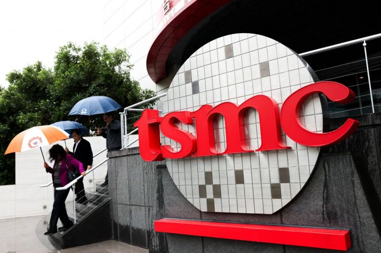
Taiwan's TSMC, the world's number one semiconductor foundry market leader, has started operating new factories one after another since the beginning of the year. Industry experts analyze that TSMC has launched a full-scale 'speed race' this year to firmly maintain its leading position.
According to foreign media and industry sources on the 3rd, TSMC began pilot production of 2nm (nanometer, one hundred millionth of a meter) process using about 5,000 semiconductor wafers at its factory in the Hsinchu Science Park in Taiwan at the start of the new year. This is said to be a pilot (standardization) type production conducted in some lines, not formal production based on customer orders.
Industry insiders interpret that through this pilot production, TSMC aims to showcase its technological capabilities to gain customer trust while simultaneously putting pressure on competitors. TSMC has announced an ambitious goal to fulfill orders from major clients such as Nvidia through the 2nm fine process starting this year.
Foundry processes are becoming increasingly detailed, approaching the 2nm stage. Not only TSMC but also Samsung Electronics and Japan's Rapidus are focusing all efforts on mass production of semiconductors using the 2nm process this year. Through this trial production, TSMC appears to demonstrate its technological superiority and determination to stay ahead in the competition.
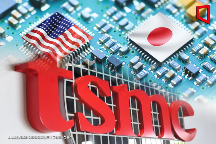
In addition to the 2nm pilot production, TSMC is accelerating the operation of its first factory established in Kumamoto Prefecture, Kyushu, Japan. The factory, which opened in February last year, is scheduled to start formal semiconductor production from this month, about 11 months after opening. This factory produces 12?16nm and 22?28nm semiconductors used in smartphones, automobiles, and various industrial devices, and is reported to have a system capable of producing 55,000 wafers per month based on 300mm wafers.
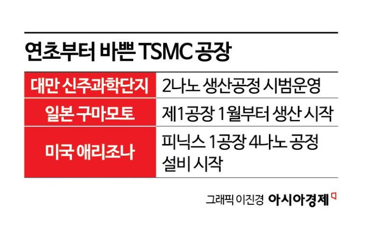
The factory located in Phoenix, Arizona, USA, will also begin semiconductor production from the first quarter of this year. According to local media, TSMC started preparing for mass production of wafers using advanced 4nm process technology in the Phase 1 (1A) process area of Phoenix Plant 1 (P1) from the end of last year. To this end, about 500 employees from the Taiwan headquarters were urgently dispatched to the site to install advanced specialized equipment. This emergency measure appears to have been taken because the work speed was judged to be slow with only local personnel. TSMC plans to complete preparations so that this factory can be fully operational by mid-year and fulfill orders from major clients such as Apple, Nvidia, AMD, and Qualcomm.
Industry analysts suggest that not only the intensifying foundry competition but also the recent rapid rise of Broadcom, which could reshape the artificial intelligence (AI) chip market, have influenced this situation.
Broadcom, which has mainly produced low-cost communication equipment chips such as Wi-Fi and Bluetooth, has recently emerged as a strong competitor to Nvidia by manufacturing advanced semiconductors supporting AI data processing. In particular, it has attracted market attention by releasing 'custom AI chips (ASIC)' tailored to customer demands. Riding on this growth, Broadcom's market capitalization surpassed $1 trillion for the first time on December 13 last year (local time).
To counter Broadcom, Nvidia is reportedly preparing various measures, including expanding production and supply of its next-generation AI chip 'Blackwell.' In this process, TSMC, which virtually monopolizes the manufacturing of Nvidia's AI chips, is likely compelled to accelerate factory operations.
© The Asia Business Daily(www.asiae.co.kr). All rights reserved.


