Ultra-fine System Semiconductor Devices and Equipment Demonstration
"Will Serve as a Stepping Stone to Strengthen the Competitiveness of Semiconductor Companies in the Region"
Pyeongtaek City in Gyeonggi Province is partnering with the Korea Nano Technology Institute to promote the establishment of a testbed for next-generation semiconductor equipment testing.
On the 4th, Pyeongtaek City announced that it will actively promote the "National Advanced Strategic Industry Specialized Complex Cooperation Support Project" implemented by the Ministry of Trade, Industry and Energy in collaboration with the Korea Nano Technology Institute.
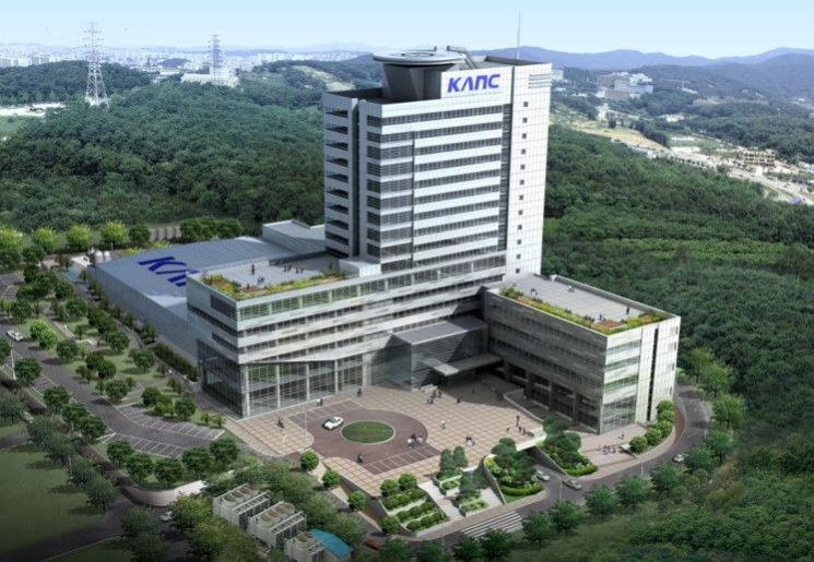 Exterior view of the Korea Nano Technology Institute located in Gwanggyo Technovalley, Suwon. Pyeongtaek City is collaborating with the institute to establish a test bed for securing advanced semiconductor materials and equipment demonstration technologies. Provided by Pyeongtaek City
The project aims to enhance the technological capabilities of semiconductor companies and secure demonstration technologies for semiconductor materials and equipment. The city explained that this project, which has been continuously pursued since the designation of the National Advanced Strategic Industry Specialized Complex last year, is now bearing fruit.
The project will be carried out over five years, with a total investment of 6 billion KRW, including 4.2 billion KRW in national funds and 1.8 billion KRW in in-kind contributions. The first phase of the project will proceed until June next year, followed by an evaluation to connect to the second phase. The final project completion target is December 2028. The city plans to review project outcomes at each stage and adjust the project direction accordingly.
The project is led by the Korea Nano Technology Institute, aiming to establish a testbed for artificial intelligence (AI) and sub-1nm ultra-fine system semiconductor devices and equipment. The testbed construction will utilize five new semiconductor process equipment within the Korea Nano Technology Institute's fab, along with approximately 170 existing pieces of equipment owned by the institute. Through this, prototype production support and corporate technology assistance will be provided, helping local semiconductor companies to commercialize next-generation semiconductor technologies early.
Before advancing to the second phase, the city plans to identify research and development (R&D) demands from local semiconductor companies and prioritize supporting projects using the testbed equipment. To this end, discussions are underway to establish a specialized center linking the specialized complex and the Korea Nano Technology Institute.
A city official stated, "This testbed construction project will serve as a stepping stone to enhance the technological capabilities and market competitiveness of local semiconductor companies," adding, "Through the cooperative system with the Korea Nano Technology Institute, we will ensure that Pyeongtaek City becomes a global hub for the semiconductor industry."
Meanwhile, the Korea Nano Technology Institute is a public semiconductor-related institution under the Ministry of Science and ICT, located in the Gwanggyo Techno Valley in Suwon. It was established to enhance national competitiveness in nanotechnology by building research and development and support systems in the fields of nano devices and compound semiconductors.
© The Asia Business Daily(www.asiae.co.kr). All rights reserved.
![User Who Sold Erroneously Deposited Bitcoins to Repay Debt and Fund Entertainment... What Did the Supreme Court Decide in 2021? [Legal Issue Check]](https://cwcontent.asiae.co.kr/asiaresize/183/2026020910431234020_1770601391.png)


