A next-generation semiconductor packaging technology that can simultaneously achieve high productivity and cost reduction has been developed in South Korea.
The Korea Institute of Machinery and Materials (KIMM) announced on the 26th that Research Fellow Junyeop Song and Dr. Jaehak Lee's research team at the Semiconductor Equipment Research Center of the Autonomous Manufacturing Research Institute, in collaboration with Hanwha Precision Machinery Co., Ltd., Cressem Co., Ltd., MTI Co., Ltd., and Nepes Co., Ltd., have developed core foundational and practical technologies to realize semiconductor packaging on large-area panels.
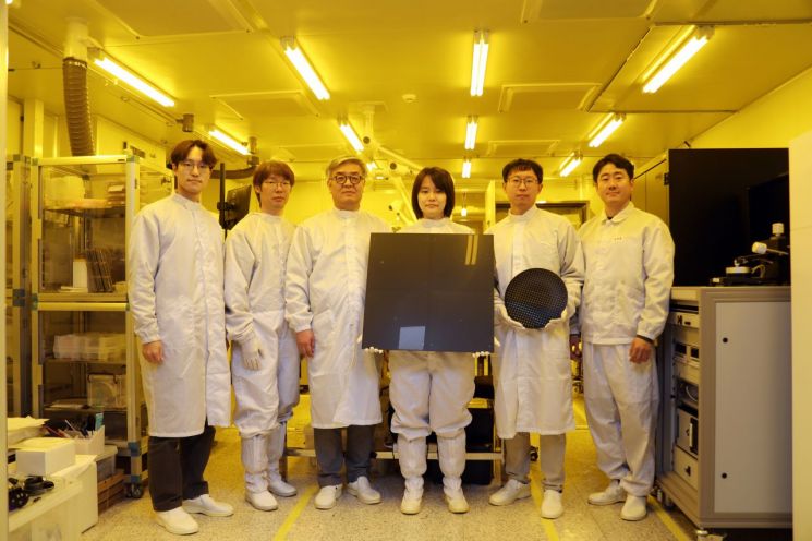 Research team led by Research Fellow Junyeop Song at the Semiconductor Equipment Research Center, Korea Institute of Machinery and Materials. Provided by Korea Institute of Machinery and Materials
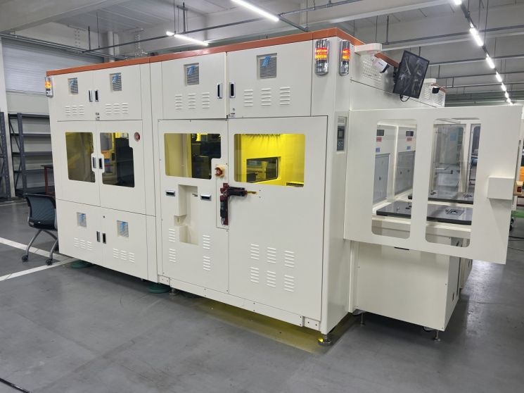
First, the research team maximized productivity by utilizing large-area square panels (600 mm × 600 mm) instead of circular (300 mm) ones. They also integrally developed and applied bonding equipment capable of producing over 10,000 chips per hour with precision within ±5 μm, and high-speed large-area inspection equipment with a resolution of 1?2 μm.
In this process, FO-PLP (Fan-Out Panel Level Packaging) bonding and inspection equipment, as well as process and material technologies, were utilized. FO-PLP is a technology that arranges semiconductor chips on large-area panels for packaging. Unlike the existing FO-WLP (Fan-Out Wafer Level Packaging) technology, which packages at the wafer level, FO-PLP uses large-area panels, offering relatively higher productivity but requiring technically challenging processes.
FO-PLP technology involves chip redistribution on large-area panels, which can cause chip adhesive step differences, rearrangement errors during adhesion, and die shift errors due to differences in thermal expansion coefficients between materials during molding. Above all, if errors accumulate at each stage, the package yield decreases.
However, the integrated artificial intelligence inspection and correction technology developed by the research team reduces die shift errors in FO-PLP, improving yield and productivity.
The team maintained die shift levels within approximately ±5 μm, achieving stable precision. This represents an improvement of over 30% in precision compared to existing technologies. Securing high precision through high-speed die shift inspection and correction technology also increased productivity by more than 30% compared to leading overseas companies.
The research team emphasized that productivity was improved by 6.5 times compared to the existing 300 mm FO-WLP, significantly reducing package manufacturing costs. In the future, by miniaturizing the line width to below 7 μm, which is the world's highest level, it is expected to be applicable to high-performance high-end packages.
Research Fellow Junyeop Song of KIMM stated, "The FO-PLP market is a high-growth sector predicted to have an average annual growth rate of 30% over the next five years," adding, "FO-PLP technology is expected to lead the semiconductor package market, which is anticipated to reach $50 billion by 2030."
Meanwhile, on the same day, KIMM signed a business agreement at the Ruby Hall of EL Tower in Seoul with the Korea Semiconductor Research Association, Hanwha Precision Machinery, Cressem, and MTI to commercialize next-generation semiconductor FO-PLP technology.
© The Asia Business Daily(www.asiae.co.kr). All rights reserved.


