Revealed in the 'SK AI Summit 2024' Keynote
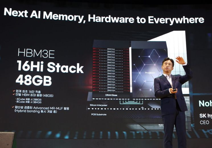
World's Largest 48GB Capacity
16 Layers Surpass Previous 12 Layers as the Highest Tier
Kwack No-jeong, CEO and President of SK Hynix, officially announced for the first time at the 'SK AI Summit 2024' held on the 4th at COEX in Samseong-dong, Seoul, that the company is currently developing a 16-stack HBM3E with 48GB, a next-generation high-bandwidth memory (HBM). The 48GB capacity is the largest among existing HBMs, and the 16-stack surpasses the previous maximum of 12 stacks.
 Kwak No-jeong, President and CEO of SK Hynix, is delivering the keynote speech titled "The New Journey of Next-Generation AI Memory, Beyond Hardware to Everyday Life" at the 'SK AI Summit 2024' held on the 4th at COEX in Samseong-dong, Seoul. Photo by SK Hynix
President Kwack stated, "We are currently preparing various 'world first' products that we have developed and mass-produced first in the world, and we are planning 'beyond best' products with the highest competitiveness." He added, "We expect the 16-stack market to open in earnest, and to prepare for this, we are developing a 48GB 16-stack HBM3E to secure technological stability, with plans to provide samples to customers early next year."
He continued, "To produce the 16-stack HBM3E, we will utilize the 'Advanced MR-MUF' process, which has proven mass production competitiveness in our 12-stack products, and as a backup, we are also developing hybrid bonding technology." MR-MUF (Mass Reflow-Molded Under Fill) is a process where, after stacking semiconductor chips, a liquid protective material is injected and solidified in the space between chips to protect the circuits. Compared to the method of laying film-type materials each time a chip is stacked, this process is more efficient and is also evaluated to be effective for heat dissipation.
President Kwack also explained through internal analysis that the 16-stack HBM3E shows an 18% performance improvement in learning tasks and a 32% improvement in inference tasks compared to the 12-stack product. With the AI accelerator market for inference expected to grow, he expressed expectations that the 16-stack HBM3E will further solidify the company's top position in AI memory.
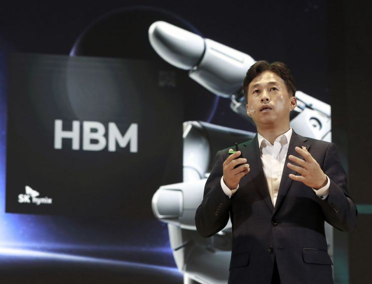 Kwak No-jeong, President and CEO of SK Hynix, is delivering the keynote speech titled "The New Journey of Next-Generation AI Memory, Beyond Hardware to Everyday Life" at the 'SK AI Summit 2024' held on the 4th at COEX, Samseong-dong, Seoul. Photo by SK Hynix
In addition, President Kwack mentioned that SK Hynix is developing the 'LPCAMM2' module, which is expected to be used in PCs and data centers in the future, boasting low power consumption and high performance, and is also producing 1cnm-based LPDDR5 and LPDDR6. Furthermore, in NAND, the company is preparing PCIe 6th generation SSDs, high-capacity QLC-based eSSDs, and UFS 5.0.
SK Hynix has also planned to introduce logic processes into the 'Base Die' starting from HBM4. The base die is the die connected to the GPU that controls the HBM. The mass production and supply schedule for HBM4 may be advanced. SK Group Chairman Chey Tae-won revealed in his keynote speech at the event that NVIDIA, SK Hynix's largest customer, requested to advance the supply of HBM4 by six months from the original schedule, and CEO Kwack responded, "We will give it a try." Originally, SK Hynix planned to mass-produce HBM4 in the second half of next year.
© The Asia Business Daily(www.asiae.co.kr). All rights reserved.


