Professor Yoo Jung-woo's Team Develops Data Storage Memory Device for Low-Power M-RAM
Dr. Choi Jong-hyun as First Author, with Participation from Drs. Park Jung-min, Kim Kyung-hwan, and Kim Choong-hyun
A new concept memory device that controls power consumption and heat generation of MRAM semiconductors has been developed.
The research team led by Professor Jungwoo Yoo from the Department of Materials Science and Engineering at UNIST (President Jongrae Park) proposed an MRAM (magnetoresistive random-access memory) device structure that can store data in memory with low power consumption and experimentally demonstrated it. The results were published in the international academic journal Nature Communications on the 10th.

MRAM is a next-generation memory that combines the advantages of NAND flash and DRAM. It has non-volatility like NAND flash, meaning data is not lost when the power is turned off, and it has speeds comparable to DRAM. It has been partially commercialized in fields requiring safety and fast data reading and writing.
This MRAM uses current to write and erase data in memory. When the magnetization directions of the two magnetic layers constituting the memory device are parallel, the resistance value is low, and when in an antiparallel state, the resistance value is high. Data is stored as 0 and 1 according to these parallel and antiparallel states. To change the magnetization direction of the magnetic layers, a current above the threshold current must flow, and the power consumption and heat generation occurring at this time were problematic.
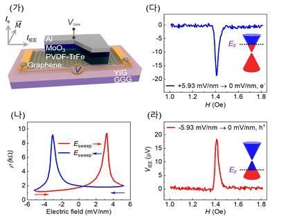
On the other hand, the memory device developed by the research team can write information to the memory using only voltage pulses. This device has a structure where graphene is sandwiched between the magnetic insulator YIG and the ferroelectric PVDF-TrFE. When a voltage pulse is applied, the direction of current flowing through the graphene changes. Data 0 and 1 are stored according to this direction.
The developed memory device applies physical theories such as the inverse Edelstein effect and ferromagnetic resonance phenomena. The principle is that the spin current injected into graphene by the ferromagnetic resonance of the magnetic insulator is converted into charge current by the inverse Edelstein effect. The current direction can be changed by applying a voltage pulse to the ferroelectric. When the voltage pulse changes the polarity of the ferroelectric, the Fermi level of graphene shifts. Depending on the Fermi level, the direction of current flowing through graphene changes.
Professor Jungwoo Yoo explained, “This research provides a breakthrough to drastically reduce heat generation and energy consumption and solve the power consumption problem of exponentially increasing AI semiconductor devices.”
Dr. Jonghyun Choi from the Department of Materials Science and Engineering at UNIST participated as the first author in this research, along with Dr. Jungmin Park (affiliated with KAIST), an alumnus of the Department of Materials Science and Engineering at UNIST, Professor Kyunghwan Kim from Yonsei University, and Dr. Choonghyun Kim from KIAS.
The research was conducted with support from the National Research Foundation of Korea’s Next-Generation Intelligent Semiconductor Technology Development Project, Nano and Materials Technology Development Project, and Basic Research Project.
© The Asia Business Daily(www.asiae.co.kr). All rights reserved.


