Product Training Session at Samsung Electronics Press Room on the 22nd
Samsung Electro-Mechanics announced plans to expand the proportion of high-value-added flip chip ball grid array (FCBGA) products, including servers, artificial intelligence (AI), automotive electronics, and networks, to over 50% within two years. This reflects their ambition to establish a strong presence in the semiconductor substrate market, currently dominated by Japan and Taiwan.
On the 22nd, Samsung Electro-Mechanics held a product learning seminar titled 'Semiconductor Substrate FCBGA Edition' at the Samsung Electronics press room in Taepyeong-ro, Seoul, where they made this announcement.
Semiconductor substrates serve to transmit electrical signals between semiconductors and main substrates, while also protecting semiconductors from external shocks. If semiconductor chips are likened to the brain, semiconductor substrates can be compared to the bones protecting the brain and the nerves and blood vessels that connect the information transmitted from the brain to various organs.
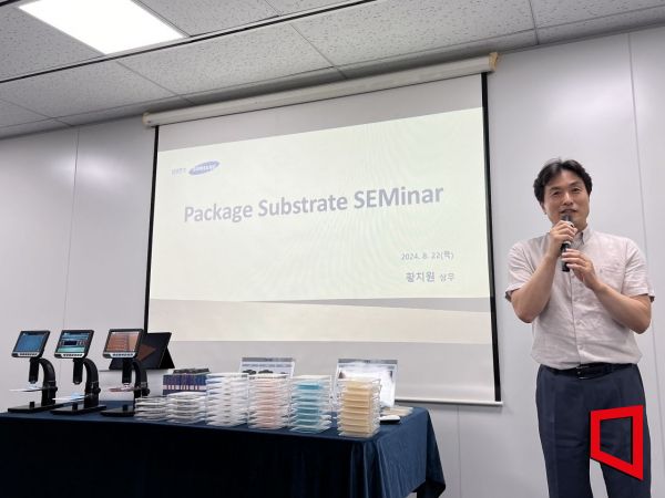 Hwang Chi-won, Executive Director and Head of Package Development Team at Samsung Electro-Mechanics, is presenting at the product training session held at the Samsung Electronics press room on the afternoon of the 22nd.
 [Photo by Han Ye-ju]
Hwang Chi-won, Executive Director and Head of the Package Development Team at Samsung Electro-Mechanics, who presented at the event, explained, "Semiconductor chips need to be connected to the main substrate, but the circuits on the main substrate cannot be made as fine as those on the semiconductor. The spacing between terminals on semiconductor chips is 100 μm (micrometers), roughly the thickness of an A4 sheet, whereas the spacing between terminals on the main substrate is about 350 μm, approximately four times larger. Therefore, a bridging component is needed to connect the semiconductor chip and the main substrate, and this is the semiconductor substrate."
Semiconductor substrates are growing mainly in industries such as 5G antennas, ARM CPUs (central processing units), servers, automotive electronics, and networks. According to market research firm Prismark, the semiconductor substrate market size is expected to grow steadily at an average annual rate of about 14%, from 4.8 trillion KRW in 2024 to 8 trillion KRW in 2028.
Among semiconductor substrates, demand for FCBGA is expected to increase sharply due to the rising demand for high-performance semiconductors driven by recent AI technologies. FCBGA is a package substrate that connects semiconductor chips and substrates via flip chip bumps, enhancing electrical and thermal characteristics. It is considered the most technologically challenging product among semiconductor substrates. Globally, fewer than 10 companies can manufacture FCBGA, with Japan's Ibiden and Shinko Electric, and Taiwan's Unimicron leading the market. Based on 2022 sales, Japanese and Taiwanese companies accounted for 69% of the FCBGA market share, while Korean companies held about 10%.
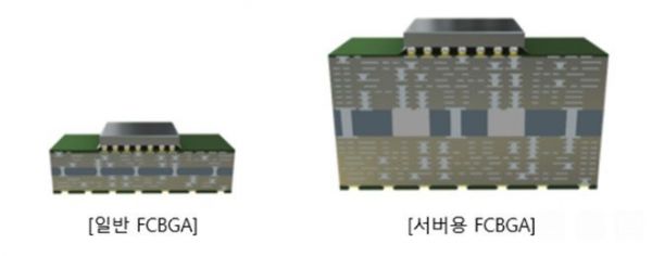
Executive Director Hwang stated, "CPUs and GPUs (graphics processing units) for servers require mounting multiple semiconductor chips on a single substrate to meet demands for enhanced computing power and connection signal speed. Therefore, server FCBGA substrates are more than four times larger in area and have more than twice the number of layers?over 20 layers?compared to general PC FCBGA. Consequently, server FCBGA is a challenging field for latecomers due to the need for manufacturing technology to improve product reliability and production yield associated with large substrate size and high multilayer count, as well as the establishment of dedicated facilities."
Samsung Electro-Mechanics explained that since successfully mass-producing server FCBGA for the first time domestically in October 2022, they have been supplying products to leading global companies with differentiated technology. Executive Director Hwang emphasized, "Although we are latecomers compared to global competitors in the FCBGA field, we are leading in capacity, technology, and power. We are strengthening cooperation with customers by securing key technologies required in the next-generation semiconductor substrate market, such as ultra-large area technology over 110 mm, ultra-high multilayer technology exceeding 26 layers, EPS technology that embeds passive components within the package substrate to enhance semiconductor performance, and technology that directly implements ultra-fine circuits on substrates to mount various silicon devices on a single package substrate, thereby boosting performance."
Investment is also ongoing. To maintain a technological lead in the semiconductor substrate field, Samsung Electro-Mechanics has invested 1.9 trillion KRW to operate new advanced high-end product mass production bases in Busan and Vietnam. In particular, the Samsung Electro-Mechanics Vietnam plant applies a smart factory system operating an intelligent manufacturing system based on an automated logistics system and advanced manufacturing environment to produce products stably.
As a result, in July, Samsung Electro-Mechanics signed a supply contract for high-performance computing (HPC) server FCBGA with global semiconductor company AMD and began mass production. Executive Director Hwang expressed confidence, saying, "(Besides AMD,) we are communicating with various customers," and "All customers worldwide are our targets."
He added, "As the first domestic company to mass-produce server FCBGA, Samsung Electro-Mechanics is focusing on next-generation substrate development and strengthening competitiveness in the semiconductor substrate business," emphasizing, "We plan to secure more than 50% of high-value-added FCBGA product share by 2026 by focusing on the high-end semiconductor substrate market for high-performance servers and networks driven by cloud market growth, as well as autonomous driving."
© The Asia Business Daily(www.asiae.co.kr). All rights reserved.

![Clutching a Stolen Dior Bag, Saying "I Hate Being Poor but Real"... The Grotesque Con of a "Human Knockoff" [Slate]](https://cwcontent.asiae.co.kr/asiaresize/183/2026021902243444107_1771435474.jpg)


