Achievements through collaboration with domestic DSP companies
Contribution to Korea Fabless support system ecosystem
Expansion of MPW service to 35 sessions next year
Samsung Electronics shared the achievements of strengthening the domestic system semiconductor ecosystem through its foundry (semiconductor contract manufacturing) event and unveiled future support plans.
The company secured a turnkey service for an AI accelerator based on a 2-nanometer process from a Japanese artificial intelligence (AI) company through collaboration with a domestic design solution provider (DSP). Moving forward, Samsung plans to support advanced and specialty process technologies for domestic fabless (semiconductor design) companies while increasing their opportunities for prototype production.
"Providing the Most Needed AI Solutions to Domestic Customers"
On the 9th, Samsung Electronics held the Samsung Foundry Forum and SAFE Forum 2024 at COEX in Seoul. The theme of the Foundry Forum was 'Empowering the AI Revolution,' while the SAFE Forum was held under the theme 'AI: Exploring Possibilities and Future.'
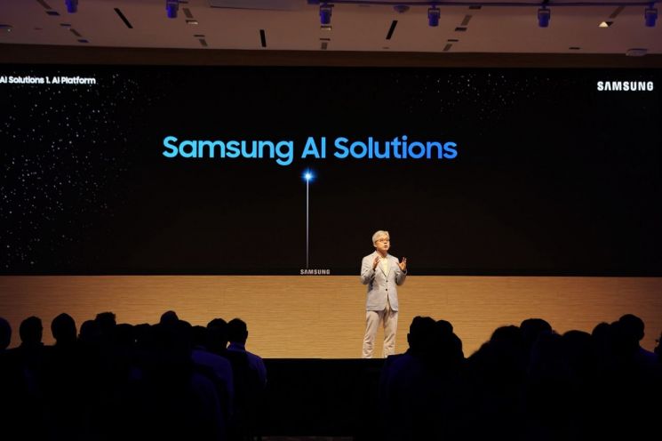 On the 12th of last month (local time), Choi Si-young, President of Samsung Electronics Foundry Business Division, delivered the keynote speech at the 'Samsung Foundry Forum 2024' held in Silicon Valley, USA /
 On this day, Samsung Electronics showcased its foundry-exclusive process technology, manufacturing competitiveness, ecosystem, and system semiconductor design solutions centered on AI. A total of 35 partner companies in DSP, intellectual property (IP), electronic design automation (EDA), and testing and packaging (OSAT) fields set up booths to present solutions supporting Samsung Foundry customers.
Choi Si-young, President of Samsung Electronics Foundry Business Division, said in the keynote speech, "Samsung Electronics supports various specialty process technologies in addition to leading-edge processes to collaborate with domestic fabless customers." He added, "Through the fusion of specialty solutions such as BCD, which improves AI power efficiency, and high-sensitivity sensor technology that enhances edge device accuracy, we will provide the AI solutions most needed by customers."
Specialty process technology is used in processes to implement specific functions such as embedded memory and image sensors. The BCD process integrates analog signal control (Bipolar), digital signal control (CMOS), and high-voltage management (DMOS) transistors into a single chip, mainly used for power semiconductor production.
Japan's 'Preferred Networks' Secures AI Accelerator Turnkey Order
At this forum, Samsung Electronics presented differentiated strategies such as integrated AI solution turnkey services tailored to customer demands, leveraging its strengths as an integrated device manufacturer (IDM) with foundry, memory, and packaging capabilities.
In particular, the company’s strategy is to strengthen leading-edge process services based on next-generation transistor structures, such as gate-all-around (GAA) processes, and 2.5D packaging technology competitiveness to realize low-power, high-performance semiconductors suitable for AI chips.
Results are already becoming visible. Samsung Electronics secured a turnkey service based on cutting-edge processes in collaboration with domestic DSP company Gaonchips. The company plans to mass-produce AI accelerator semiconductors based on Japan's Preferred Networks (PFN) 2-nanometer (SF2) process using advanced 2.5D (I-Cube S) packaging.
PFN, a Japanese AI company, develops related software and hardware technologies. It operates a vertically integrated AI value chain business covering related chips, supercomputers, and generative AI-based models in the deep learning field.
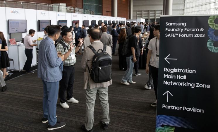 The scene at the 'Samsung Foundry·SAFE Forum 2023' held last July at COEX, Samseong-dong, Seoul / [Photo provided by Samsung Electronics]
Samsung Electronics plans to support domestic fabless companies in expanding their influence in high-performance computing (HPC) and AI fields by collaborating with DSP partners. The company supports domestic customers in utilizing the latest process technologies and operates a multi-project wafer (MPW) service for prototype production.
Customers using the MPW service can place multiple designs on a wafer for testing, reducing manufacturing costs while developing highly refined semiconductors. Samsung Electronics’ total MPW service count this year is 32 times, covering processes from 4 nanometers to 130 nanometers, which is about a 10% increase compared to last year.
Samsung plans to increase the number of MPW services to 35 times next year. Especially for the 4-nanometer process, which has high demand from domestic fabless and DSP companies, the MPW service will be operated one more time than this year to support the domestic advanced semiconductor ecosystem in HPC and AI fields.
Japan and Europe Foundry Forums Scheduled for Second Half of the Year
Samsung Electronics also provided networking opportunities among partners and held discussions on strengthening cooperation for innovation. Three domestic fabless companies?Telechips, Above, and Rebellion?shared successful cooperation achievements, visions with Samsung Electronics, and fabless industry trends through presentations at the Samsung Foundry Forum sessions.
At the SAFE Forum, Samsung Electronics and domestic and international partners focused on introducing AI semiconductor design infrastructure, including 2.5D and 3D chiplet design technologies, IP portfolios, and methodologies for verifying and optimizing designs.
Earlier, Samsung Electronics shared the results of the first workshop of the advanced packaging consortium (Multi-Die Integration Alliance) with partners at the Foundry Forum held last month in Silicon Valley, USA. The company emphasized the high potential for next-generation high-performance and high-bandwidth semiconductor implementation using advanced process technology, design infrastructure, and packaging technology.
Meanwhile, Samsung Electronics holds Foundry Forums and SAFE Forums annually at major global hubs. After hosting events in the US and domestically, the company plans to hold additional events in Japan (Tokyo) and Europe (Munich, Germany) in the second half of the year.
© The Asia Business Daily(www.asiae.co.kr). All rights reserved.


