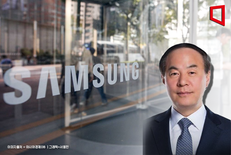
First Organizational Restructuring After Vice Chairman Jeon Young-hyun's Appointment
Focus on Developing HBM3E and HBM4
Reorganization of Advanced Packaging AVP Development Team
Enhancing Synergy at Equipment Technology Research Institute
Samsung Electronics has carried out a major organizational restructuring, including the establishment of a High Bandwidth Memory (HBM) development team. This comes just over a month after Vice Chairman Jeon Young-hyun took charge of Samsung Electronics' Device Solutions (DS) division. The move is interpreted as an effort to strengthen HBM technology leadership and competitiveness amid a surge in HBM demand driven by the expansion of the artificial intelligence (AI) market.
According to industry sources on the 5th, Samsung Electronics' DS division implemented an organizational restructuring the day before, centered on the creation of the HBM development team. Although the company has had a dedicated HBM organization since 2015, this is the first time it has been included in the official organizational chart. It is reported that all personnel related to HBM, previously scattered under various business teams, will be consolidated.
The new head of the HBM development team is known to be Vice President Son Young-soo, an expert in high-performance DRAM product design. He joined the DRAM design team under the DRAM development office in 2003 and has been responsible for designing and planning high-performance DRAM products such as HBM and Double Data Rate (DDR) 5.
The newly established HBM development team is expected to focus on the development of HBM3, HBM3E, as well as next-generation HBM4 technology.
With this organizational restructuring, Samsung Electronics plans to further strengthen its dedicated HBM organization and intensify efforts in next-generation research and development (R&D). Regarding NVIDIA quality testing, completing certification work and delivering both 8-stack and 12-stack HBM3E in the second half of the year is one of Vice Chairman Jeon's tasks. The market expects that once testing is completed within this year, full-scale supply will begin from next year. Song Jae-hyuk, CTO and President of the DS division, recently commented on the quality testing, saying, "We are working hard" and "There will be good results."
In addition, the Advanced Packaging (AVP) business team, which has been responsible for semiconductor packaging technology development, has been reorganized into the AVP development team and placed directly under Vice Chairman Jeon. This is intended to proactively secure new packaging technologies such as 2.5D and 3D. As competition intensifies in 2.5D packaging, which vertically stacks processors such as HBM and GPUs, as well as 3D packaging that stacks processors on top of HBM, the role of the AVP development team is expected to grow. The Equipment Technology Research Institute under the CTO, responsible for semiconductor production facilities and process development, will also be reorganized.
© The Asia Business Daily(www.asiae.co.kr). All rights reserved.


