Scheduled for the 9th of next month... Major AI Strategies Unveiled
Introduction of One-Stop AI Solutions and Collaboration with Fabless Companies
Samsung Electronics will hold a Foundry Forum next month and work with domestic fabless companies (fabless: semiconductor design specialists) to strengthen the artificial intelligence (AI) chip and system semiconductor ecosystem.
According to industry sources on the 28th, Samsung Electronics will hold the 'Samsung Foundry Forum 2024' and 'SAFE (Samsung Advanced Foundry Ecosystem) Forum 2024' at COEX in Gangnam-gu, Seoul on the 9th of next month.
The 'Samsung Foundry Forum' is an event to introduce semiconductor process technology roadmaps to customers and promote the competitiveness of the foundry (semiconductor contract manufacturing) business. It is held sequentially in South Korea, the United States, Japan, and Europe. The 'SAFE Forum,' where partner companies announce technology collaborations and network with each other, has also been held since October 2019.
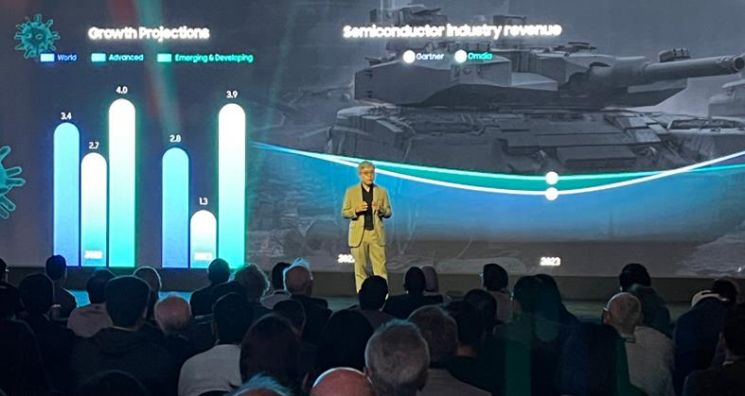
At this Foundry Forum, Choi Si-young, President of Samsung Electronics Foundry Division, will deliver the keynote speech, and Lee Jang-gyu, CEO of Telechips, Park Ho-jin, Vice President of Above Semiconductor, and Oh Jin-wook, Chief Technology Officer (CTO) of Rebellion, will give presentations on automotive semiconductors, cooperation with Samsung Foundry, and artificial intelligence (AI) semiconductors.
Additionally, executives from Samsung Electronics' Device Solutions (DS) division will hold presentation sessions related to AI solutions, design platforms, business, and customers.
This event is expected to reveal a large number of Samsung Electronics' AI semiconductor-related technology strategies. In particular, it plans to emphasize a 'one-stop service' for AI chip production, including foundry, memory, and advanced package business (AVP: Advanced Packaging). It will also introduce achievements in AI and low-power semiconductor fields with major domestic fabless companies and announce future cooperation plans.
Earlier, on the 13th, Samsung Electronics announced at the Foundry Forum held in Silicon Valley, USA, that it plans to further strengthen the one-stop turnkey service for AI chip production, providing foundry, memory, and advanced packaging as a 'one team' by 2027.
Through cooperation among the three semiconductor business sectors, the company aims to present integrated AI solutions with strengths such as high performance, low power consumption, and high bandwidth, contributing to simplifying customers' supply chains. By 2027, it plans to introduce the 2-nanometer (nm; 1 nm is one billionth of a meter) process 'SF2Z,' which applies 'Backside Power Delivery Network' (BSPDN) technology to the 2-nanometer process.
Currently, Samsung Electronics has been mass-producing the world's first 3-nanometer process with next-generation transistor Gate-All-Around (GAA) technology since 2022. It plans to start mass production of the second-generation 3-nanometer process in the second half of this year.
President Choi Si-young said, "The most important thing in the AI era is high-performance, low-power semiconductors that enable AI implementation," adding, "We will provide one-stop AI solutions that customers need in the AI era through GAA process technology optimized for AI semiconductors and optical device technology."
At the SAFE Forum, Gye Jong-wook, Vice President and Head of Design Platform Development at Samsung Electronics Foundry Division, and Shanka Krishnamurthy, General Manager of Synopsys EDA Group, will attend to discuss the development direction of chip and system design technologies needed in the AI era.
© The Asia Business Daily(www.asiae.co.kr). All rights reserved.


