Two Projects Including 'Advanced Semiconductor Packaging' and 'K-Cloud Development Using AI Semiconductors' Pass Preliminary Feasibility Study
The government has decided to invest 677.5 billion KRW in national research and development (R&D) funding to promote 'de-NVIDIA' in the artificial intelligence (AI) semiconductor sector and to enhance South Korea's semiconductor packaging technology, which lags behind competing countries.
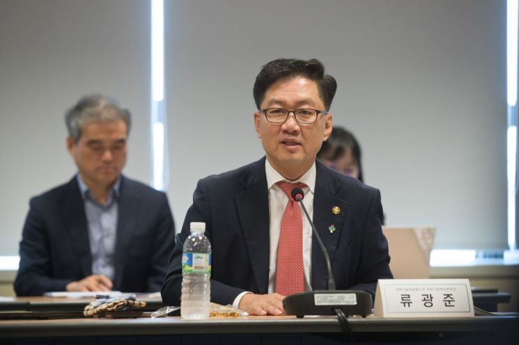 Ryu Gwang-jun, Director General of the Science and Technology Innovation Bureau at the Ministry of Science and ICT, is delivering closing remarks on the morning of the 26th at the National Science and Technology Advisory Council's main conference room in the Gwanghwamun Kyobo Building, Jongno-gu, Seoul, during the '5th National Research and Development Project Evaluation General Committee'.
On the 26th, the Ministry of Science and ICT announced at the 5th General Committee Meeting for National R&D Projects in 2024 that two projects, ‘Advanced Semiconductor Packaging’ and ‘Development of K-Cloud Using AI Semiconductors,’ have passed the preliminary feasibility study.
The K-Cloud technology development project using AI semiconductors, promoted by the Ministry of Science and ICT, aims to replace NVIDIA’s graphics processing units (GPUs) used in AI development. The core goals are to develop key technologies for data centers based on low-power, high-efficiency domestic AI semiconductors and to secure a sustainable AI computing infrastructure. A total budget of 403 billion KRW will be invested, with the project running for six years from 2025 to 2030.
The project plans to leverage the NPU (Neural Processing Unit) and PIM (Processing-In-Memory) semiconductors developed through the ongoing Next-Generation Intelligent Semiconductor Technology Development project and the PIM AI Semiconductor Core Technology Development project, which have already passed feasibility studies. The Ministry of Science and ICT has set a goal that by 2030, when the project concludes, the developed technology will rank within the top three worldwide in terms of learning performance efficiency and inference energy consumption efficiency among similar AI computing systems released in the market, and that more than 20% of the technology will be utilized in domestic cloud services.
Through this, the Ministry expects to enhance the competitiveness of South Korea’s system semiconductor industry, which has been heavily focused on memory semiconductors, and contribute to the expansion of domestic AI semiconductor usage and export growth.
Countries worldwide are competing to develop intelligent semiconductors that surpass existing GPUs in power consumption, efficiency, and performance. South Korea also announced the ‘AI-Semiconductor Initiative (Draft)’ at the plenary meeting of the National Science and Technology Advisory Council on April 25, which includes memory innovation through AI semiconductor development, advancement of AI semiconductors, and demonstration of AI services linked to these technologies.
The Advanced Semiconductor Packaging Leading Technology Development project submitted by the Ministry of Trade, Industry and Energy will be carried out over seven years from 2025 to 2031 with a total budget of 274.4 billion KRW.
The ‘Advanced Semiconductor Packaging Leading Technology Development project’ aims to support technology development in the rapidly advancing field of semiconductor advanced packaging to overcome the limits of semiconductor integration density and secure technological competitive advantages within the global advanced semiconductor supply chain. Comprehensive support will be provided not only for ultra-fine processes nearing their limits but also for advanced packaging leading technologies in the post-processing stage. By investing more than four times the government R&D investment of approximately 65 billion KRW made in the advanced packaging field over the past five years, the project is expected to secure key core technologies in packaging and gain competitiveness in the next-generation high value-added system semiconductor market.
Semiconductor packaging refers to the process of cutting semiconductors produced in wafer form and connecting electrical wiring to assemble them into a form that can be mounted on electronic devices. Recently, as the physical limits of integration density improvement through semiconductor process miniaturization have been reached, packaging technology that enhances semiconductor performance and integration density in the post-processing stage has gained attention.
The global advanced semiconductor packaging market is expected to grow at an average annual rate of 10% to reach 78.6 billion USD by 2028, but South Korea’s market share in the post-processing field is below 10%, which is lower than competing countries such as Taiwan, the United States, and China.
Ryu Gwang-jun, Director of the Science and Technology Innovation Headquarters, urged, “Please make every effort to ensure the smooth progress of the two major semiconductor projects that passed the preliminary feasibility study today so that South Korea can secure competitiveness and take the lead in the future semiconductor market.”
© The Asia Business Daily(www.asiae.co.kr). All rights reserved.
!["The Woman Who Threw Herself into the Water Clutching a Stolen Dior Bag"...A Grotesque Success Story That Shakes the Korean Psyche [Slate]](https://cwcontent.asiae.co.kr/asiaresize/183/2026021902243444107_1771435474.jpg)


