Samsung Foundry Forum 2024 Held in the US
2nm 'Backside Power Delivery' Introduced... Process Advancement
'AI Semiconductor Turnkey Service' Accelerates
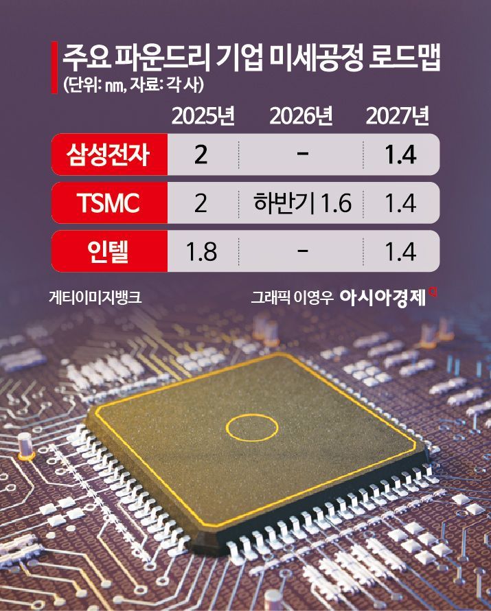
Samsung Electronics has decided to introduce the 'Backside Power Delivery Network (BSPDN)' technology, known as a 'game changer for ultra-fine processes,' for its 2㎚ (nanometer; 1㎚ = one billionth of a meter) process by 2027. 'Backside Power Delivery' is a highly advanced technology that places power lines on the back of the wafer to improve bottlenecks in power and signal lines, enabling a revolutionary implementation of ultra-fine processes. This move is seen as a strategic play to catch up with Taiwan's TSMC, a competitor in the foundry (semiconductor contract manufacturing) market. Alongside this, Samsung also expressed its intention to strengthen 'turnkey services' through collaboration among foundry, memory, and advanced package solutions.
On the 12th (local time), Samsung Electronics held the 'Samsung Foundry Forum 2024' at the Semiconductor (DS) Division Americas headquarters in San Jose, California, USA, where it announced its foundry strategy for the AI era centered on these points.
At the event, Samsung Electronics additionally unveiled 2㎚ (SF2Z) and 4㎚ (SF4U) in its existing foundry process roadmap. In particular, it announced plans to introduce the 2㎚ process applying backside power delivery technology in 2027. Applying this technology will improve efficiency compared to the existing 2㎚ process and significantly reduce the 'voltage drop' phenomenon that destabilizes current flow. This leads to enhanced performance in high-performance computing designs.
Another new process, 4㎚ (SF4U), enables 'optical shrinkage,' which makes chips smaller while improving performance compared to the existing 4㎚ process. Samsung plans to start mass production from next year.
Samsung Electronics also revealed plans to fully leverage its unique advantage as the only company possessing foundry, memory, and advanced packaging businesses. Through cooperation among these businesses, it aims to accelerate 'AI semiconductor turnkey services.' Fabless customers using Samsung’s integrated AI solutions can reduce the time required from chip development to production by about 20% compared to using foundry, memory, and packaging companies separately. Samsung plans to integrate optical devices into its AI solutions by 2027.
Choi Si-young, President of Samsung Electronics’ Foundry Business Division, said, "At a time when all technologies are undergoing revolutionary changes centered on AI, the most important thing is high-performance, low-power semiconductors that enable AI implementation," adding, "Samsung Electronics will provide a one-stop AI solution through gate-all-around (GAA) process technology optimized for AI semiconductors and optical device technology capable of high-speed data processing with low power consumption."
The event was attended by key industry experts including Rene Haas, CEO of ARM, and Jonathan Ross, CEO of Groq.
© The Asia Business Daily(www.asiae.co.kr). All rights reserved.


