Hwang Cheol-ju, Chairman of Jusung Engineering, Press Conference
"World's First Mass Production Technology for 3-5 Compound Semiconductors... Process Possible at 400°C"
Utilizing Semiconductors, Displays, and Solar Power... "Orders Will Increase"
Jusung Engineering, a domestic semiconductor equipment company, announced that it has developed the world's first mass production technology for III-V compound semiconductors. These semiconductors are made by combining elements from groups 3 and 5 of the periodic table instead of silicon, with gallium arsenide semiconductors being a representative example. They are faster than silicon materials and are expected to help improve the efficiency of next-generation semiconductor processes.
 Hwang Cheol-ju, Chairman of Jusung Engineering, is speaking at a press conference held at the Jusung R&D Center in Yongin.
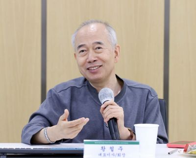
 [Photo by Jusung Engineering]
On the 5th, at a press conference held at Jusung R&D Center in Yongin, Gyeonggi Province, Hwang Cheol-joo, chairman of Jusung Engineering, stated, "We have developed technology that allows the III-V semiconductor process, which was only possible at 1000 degrees Celsius, to be done at 400 degrees Celsius," adding, "We have succeeded in developing the world's only mass production technology for III-V compound semiconductors."
III-V semiconductors have higher electron mobility than silicon and are used in LEDs, lasers, and other optoelectronic devices. They have faster switching speeds and higher frequencies than silicon semiconductors. Additionally, they have higher voltage limits, making them suitable for high-power applications.
Chairman Hwang said, "This technology can dramatically improve the efficiency of next-generation semiconductor processes such as logic (non-memory) semiconductors and micro LEDs, and we expect explosive demand from our customers," adding, "If the transfer of III-V semiconductor technology proceeds, it will have a positive impact on increasing semiconductor sales, which accounted for 75.4% of the company's revenue as of the first quarter."
He emphasized, "III-V semiconductors can be applied not only to Apple micro LEDs and Intel-developed LEDs but also represent even more advanced technology. All memory and logic semiconductor companies will use this technology, and it will be widely utilized beyond semiconductors in display and solar power industries."
Jusung Engineering is currently pursuing a spin-off in the semiconductor, display, and solar power sectors. Chairman Hwang explained that the reason for the spin-off is generally to reduce risk and increase corporate value. Given the recent difficulties in selling equipment due to U.S. sanctions on China, it was judged risky to be overly concentrated in either the semiconductor or display business. He also cited that the company’s value was being undervalued due to running the solar power business concurrently as another reason for the spin-off decision.
After restructuring its governance, Jusung Engineering has appointed Hwang Eun-seok, the chairman’s only son, as the CEO of the newly established semiconductor spin-off company. Chairman Hwang said, "He has been tentatively appointed as CEO, but it is not finalized," adding, "There is a high possibility of moving to a co-CEO system." He further stated, "For second-generation management, social respect and proven capability are necessary, so we need to observe further."
© The Asia Business Daily(www.asiae.co.kr). All rights reserved.


