Goal of Over 250 Billion KRW in Sales This Year
Semes, a domestic semiconductor and display manufacturing equipment company, announced on the 3rd that it has developed and is mass-producing next-generation bonding equipment necessary for manufacturing high-bandwidth memory (HBM) for artificial intelligence (AI).
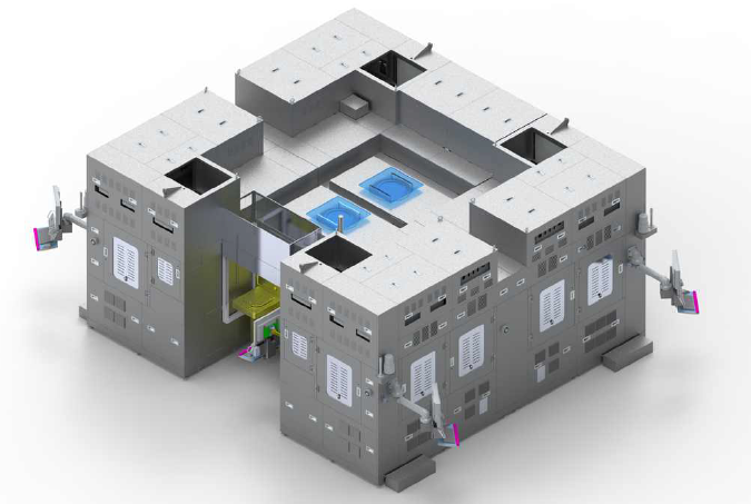
The HBM thermal compression (TC) bonder mass-produced by Semes is equipment that vertically stacks semiconductor chips made using advanced through-silicon via (TSV) technology onto wafers. It has the performance to respond to the increasing number of micro bumps (conductive protrusions) in HBM technology trends.
In particular, it achieves high stacking precision through position alignment, heat, and pressure adjustments during the bonding process. It applies a process optimized for HBM, which is manufactured using the non-conductive film (NCF) method, thereby improving productivity.
Semes recorded sales of 100 billion KRW last year through the TC bonder. This year, it aims for sales exceeding 250 billion KRW. In preparation for the ultra-fine processes that will emerge after the HBM 6th generation product, HBM4, it is developing and evaluating a hybrid bonder that stacks chips without separate connecting terminals.
Jung Tae-kyung, CEO of Semes, said, "With the development of the hybrid bonder that integrates various semiconductor process technologies, we have secured the best competitiveness in this field," and added, "We will achieve sales growth by gaining recognition for equipment quality and reliability."
© The Asia Business Daily(www.asiae.co.kr). All rights reserved.


