Analytical technology for the commercialization of two-dimensional van der Waals materials (2D van der Waals Materials) has been developed domestically. These materials are attracting attention as key substances for next-generation semiconductor technology that will replace silicon.
The National Research Foundation of Korea announced on the 2nd that Professor Jaehyun Lee's research team at Ajou University, together with Professor Dongmok Hwang at Sungkyunkwan University and Professor Taehun Kim at Chonnam National University, developed a '2D crystal scanner technology' capable of accurately analyzing the microstructure of synthesized polycrystalline two-dimensional van der Waals materials.

Two-dimensional van der Waals materials are ultra-thin film materials in a planar form with a thickness of a single atomic layer. They can maintain physical and chemical properties and stability within ultra-high-density semiconductors with nanoscale linewidths and thicknesses, making them a strong candidate to replace silicon. Graphene is also one of the two-dimensional materials.
However, to apply new materials to actual products, it is necessary to first develop technology that can accurately analyze the microstructure to understand the overall characteristics of the material.
Until now, two-dimensional van der Waals materials have been only an atomic layer thick, making it impossible to directly apply commonly used microstructure analysis methods such as X-ray crystallography and electron microscopy. For the commercialization of synthesized two-dimensional van der Waals materials, technology capable of accurately analyzing the microstructure was needed.
The technology developed by the research team overcomes these limitations, marking a significant step toward the commercialization of two-dimensional van der Waals materials.
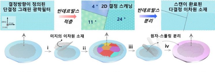
First, during the development process, the research team focused on the Moir? pattern and the resulting optical property changes that appear when different two-dimensional van der Waals materials are stacked at different angles. A Moir? pattern refers to a new pattern with a different periodicity that appears when regularly repeating patterns are overlaid.
The research team utilized single-crystal monolayer graphene, whose crystal orientation of the microstructure confirmed by the Moir? pattern and optical properties was used as an optical filter. They then stacked an unknown polycrystalline graphene synthesized on top by van der Waals forces (forces that attract neutral molecules at electrically close distances) and analyzed the changes using Raman spectroscopy.
 Schematic illustration of the '2D Crystal Scanner Technology' developed by the research team led by Professor Lee Jaehyun at Ajou University. Provided by Korea Student Aid Foundation.
As a result, it was confirmed that various microstructural information inside the unknown polycrystalline graphene was stacked at different angles with the single-crystal monolayer graphene used as the optical filter. Through this, the optical information of the misaligned microstructure could be quickly and accurately scanned and imaged.
Additionally, the analyzed specimen was cleanly separated without physical damage, like peeling off a 'Post-it,' using atomic spalling technology. Atomic spalling technology is the research team's proprietary technology that allows control of the depth and direction of cracks occurring in layered structures of two-dimensional van der Waals crystals stacked by weak van der Waals forces at the atomic thickness level.
The research team expects this achievement to be actively utilized in material fields requiring high reliability by enabling rapid and accurate analysis of the microstructure of large-area synthesized two-dimensional materials.
Professor Jaehyun Lee said, "This research achievement overcomes the limitations of existing analysis and approach methods for two-dimensional van der Waals materials, providing a non-destructive, rapid, and accurate analysis technology that will contribute to the mass production of two-dimensional van der Waals materials in the future." He added, "Currently, the research team is focusing on developing the research results into 'real-time high-speed analysis technology' applicable to mass production processes through follow-up studies."
Meanwhile, the research was conducted as part of the mid-career researcher support project in science and engineering fields promoted by the Ministry of Science and ICT and the National Research Foundation of Korea. The research results were also published online on the 4th of last month in the international materials science journal Advanced Materials.
© The Asia Business Daily(www.asiae.co.kr). All rights reserved.
![Clutching a Stolen Dior Bag, Saying "I Hate Being Poor but Real"... The Grotesque Con of a "Human Knockoff" [Slate]](https://cwcontent.asiae.co.kr/asiaresize/183/2026021902243444107_1771435474.jpg)


