Zeiss Holds Over 2,000 EUV Patents
Samsung Electronics Mass Produces 6th Generation 10nm-Class DRAM Based on EUV
Expectations for Semiconductor Performance Improvement and Production Process Optimization
Samsung Electronics Chairman Lee Jae-yong visited the ZEISS headquarters in Oberkochen, Germany, on the 26th local time and met with CEO Carl Lamprecht and other executives to discuss ways to strengthen cooperation between the two companies, Samsung Electronics announced on the 28th.
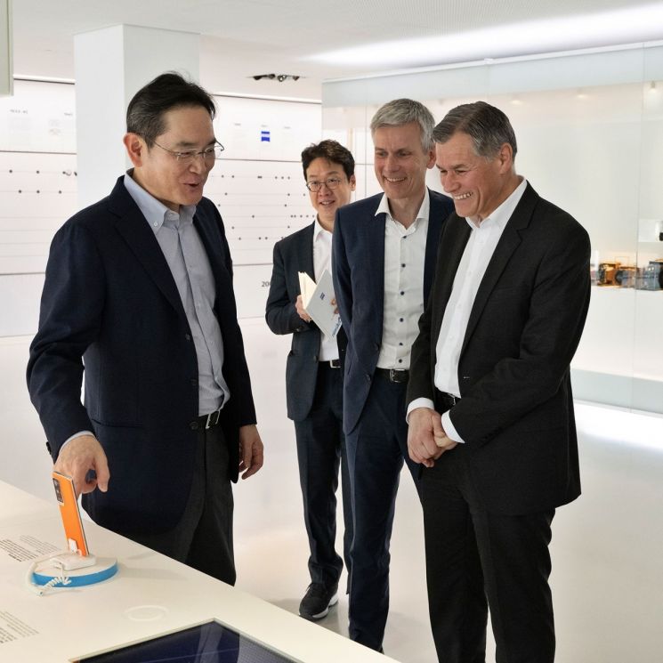
 On the 26th (local time), Samsung Electronics Chairman Lee Jae-yong, who visited the Zeiss headquarters in Oberkochen, Germany, is seen conversing with Karl Lamprecht, CEO of the Zeiss Group (far right). Photo by Samsung Electronics
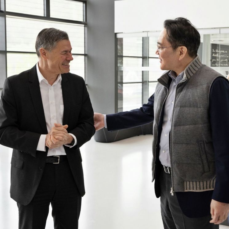
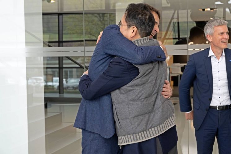 On the 26th (local time), Samsung Electronics Chairman Lee Jae-yong is seen greeting the Zeiss management during his visit to the Zeiss headquarters in Oberkochen, Germany. Photo by Samsung Electronics
Chairman Lee particularly exchanged views with ZEISS executives on semiconductor core technology trends and the mid- to long-term technology roadmaps of both companies. He then visited ZEISS’s factory to observe the production of the latest semiconductor components and equipment. Accompanying him at the ZEISS headquarters were Samsung Electronics DS Division Chief Technology Officer (CTO) Song Jae-hyuk and President of Manufacturing & Technology Nam Seok-woo, executives overseeing semiconductor production technology.
ZEISS is a global optics company holding more than 2,000 core patents related to EUV (extreme ultraviolet) technology essential for advanced semiconductor production. It exclusively supplies the optical systems installed in ASML’s EUV equipment. More than 30,000 ZEISS components are used in a single EUV machine. Samsung Electronics plans to further expand cooperation with ZEISS in the fields of future EUV technology and advanced semiconductor equipment. This partnership aims to strengthen competitiveness in both the foundry and memory businesses.
Based on its EUV technology, Samsung Electronics is leading the sub-3-nanometer ultra-fine process market in the foundry sector and plans to mass-produce 6th generation 10-nanometer class DRAM applying EUV processes within this year. Through this technological cooperation with ZEISS, Samsung expects to improve next-generation semiconductor performance, optimize production processes, and enhance yield, thereby boosting business competitiveness. ZEISS also plans to invest 48 billion KRW by 2026 to establish a research and development (R&D) center in Korea, which is expected to further strengthen the strategic cooperation between the two companies.
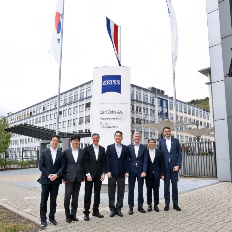 On the 26th (local time), Samsung Electronics Chairman Lee Jae-yong (center) visited the Zeiss headquarters in Oberkochen, Germany, and took a commemorative photo with Karl Lamprecht, Zeiss Group CEO (third from the left), and Andreas Pecher, Zeiss SMT (Semiconductor Manufacturing Technology) CEO (third from the right). Photo by Samsung Electronics
 On the 26th (local time), Samsung Electronics Chairman Lee Jae-yong visited the Zeiss headquarters in Oberkochen, Germany, and is seen conversing with Karl Lamprecht, CEO of Zeiss Group (far right), and Andreas Pecher, CEO of ZEISS SMT (Semiconductor Manufacturing Technology) (second from the right). Photo by Samsung Electronics
Meanwhile, Chairman Lee is making every effort to secure a leading position in the AI semiconductor market and future growth engines. In February, he met with Mark Zuckerberg, Meta CEO, who visited Korea, and prior to that, in May last year, he met with Jensen Huang, NVIDIA CEO, and in December of the same year, with Peter Wennink, ASML CEO, consecutively discussing future cooperation with top executives of global IT companies.
Building on Chairman Lee’s initiatives, Samsung Electronics continues to invest in the future to secure solid business competitiveness in the system semiconductor sector following its memory semiconductor business. Last year, Samsung Electronics achieved the largest-ever foundry order backlog and is nurturing the foundry business as a core future growth engine through maintaining technological superiority in sub-3-nanometer ultra-fine processes, diversifying customers, proactive R&D investment, bold domestic and overseas facility investments, and fostering the semiconductor ecosystem.
The mobile AP ‘Exynos 2400,’ which has improved AI performance by about 15 times compared to its predecessor, is expected to be installed in Samsung’s flagship smartphone Galaxy S24, significantly boosting sales. In the image sensor field, Samsung is rapidly closing in on the industry leader by mass-producing various products such as the ‘ISOCELL Vision 63D,’ launched in December last year. Samsung has maintained the world’s number one position in the DDI (Display Driver IC) market for 21 consecutive years. Samsung is also actively nurturing its NPU (Neural Processing Unit) business, which mimics the human brain’s neural network processing, expanding its system semiconductor business domain.
© The Asia Business Daily(www.asiae.co.kr). All rights reserved.


