Customer Supply Begins After 7 Months of Development
"We Will Strengthen Our Global No.1 Competitiveness"
SK Hynix has begun full-scale mass production of the 5th generation high-bandwidth memory (HBM) ‘HBM3E’ DRAM and will be the first to supply it to Nvidia by the end of this month. On the same day Nvidia unveiled its AI chip at a developer conference, SK Hynix announced that it would supply advanced memory to support it. Following HBM3, SK Hynix plans to solidify its leadership in the HBM market by being the first in the world to start large-scale mass production of HBM3E.
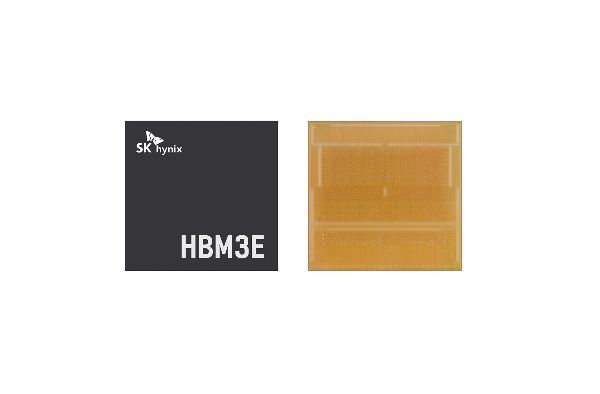
On the 19th, SK Hynix announced that it has become the first in the world to mass-produce the new ultra-high-performance AI memory product HBM3E and will begin supplying the product from the end of this month. This comes just seven months after announcing the development of HBM3E in August last year.
The company stated, "Following HBM3, HBM3E, which also delivers the highest performance currently available in DRAM, will be supplied to customers first," adding, "We will continue to maintain our competitive edge in the AI memory market."
To implement AI systems that need to process enormous amounts of data quickly, semiconductor packages must be configured by multi-connecting numerous AI processors and memory modules.
Global big tech companies that are increasing their investments in AI continue to raise the performance requirements for AI semiconductors, and SK Hynix explains that HBM3E is the optimal product to meet these demands.
According to SK Hynix’s own evaluation, the HBM3E it mass-produces boasts the world’s highest performance in all aspects required for AI memory, including speed. This product can process up to 1.18TB (terabytes) of data per second. This is equivalent to processing more than 230 Full-HD (FHD) movies (5GB each) in just one second.
Since AI memory must operate at extremely high speeds, effective heat dissipation control is also crucial. SK Hynix applied the advanced MR-MUF (Mass Reflow-Molded Underfill) process to improve heat dissipation performance by 10% compared to the previous generation.
MR-MUF is a process where, after stacking semiconductor chips, a liquid protective material is injected into the spaces between the chips and solidified to protect the circuits between them. Compared to the method of laying film-type materials each time a chip is stacked, this process is more efficient and is evaluated to be effective for heat dissipation.
Ryu Seong-su, Vice Chairman of SK Hynix, emphasized, "Through the world’s first mass production of HBM3E, we have further strengthened our product lineup leading the AI memory industry. Based on our accumulated successful HBM business experience, we will solidify customer relationships and establish our status as a ‘Total AI Memory Provider.’"
Taiwanese market research firm TrendForce predicted that this year’s wafer-based HBM production capacity will be 130,000 units per month for Samsung Electronics and 120,000 to 125,000 units per month for SK Hynix.
© The Asia Business Daily(www.asiae.co.kr). All rights reserved.


